Architecture, Engineering
& Construction
& Construction

Integrated BIM tools, including Revit, AutoCAD, and Civil 3D
Product Design
& Manufacturing
& Manufacturing

Professional CAD/CAM tools built on Inventor and AutoCAD

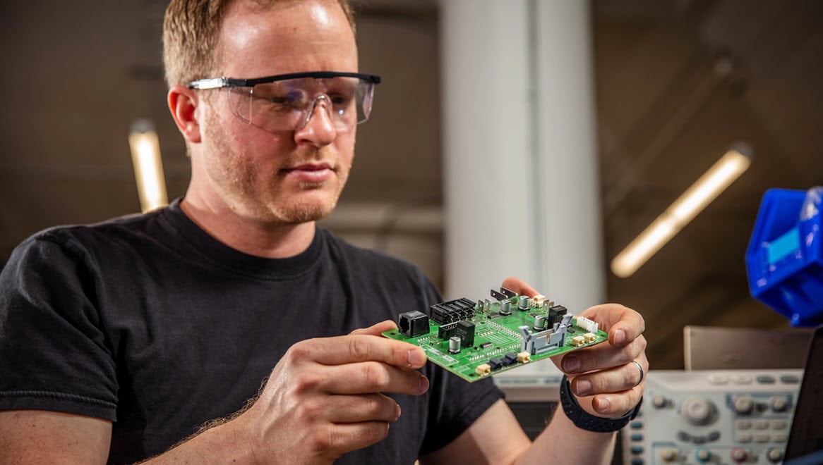
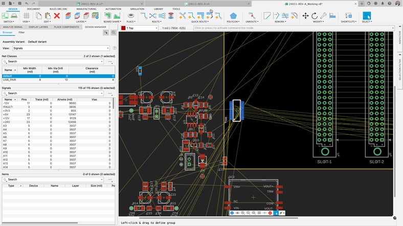
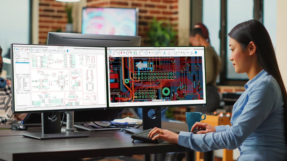
PCB design is the engineering process of creating a printed circuit board (PCB) that electrically connects and mechanically supports electronic components. PCB design includes schematic capture, PCB layout, component placement, copper trace routing and design rule validation to ensure manufacturability and performance.
PCB design software allows engineers and designers to plan, visualise and prepare the detailed layout that connects electronic components for reliable performance.
When terms like “PCB board design software” or “PCB layout tools” are used, they specifically describe the process of configuring the board’s shape, copper traces, components and preparing files for manufacturing. PCB design software helps ensure accuracy, manufacturability and efficient collaboration to turn electronic concepts into real, functional products.
PCB design refers to the full electronic design workflow, including schematics, rules and system intent. PCB board design focuses specifically on the physical layout of the board—component placement, copper routing, layers and manufacturability constraints. Modern PCB design software combines both into a single workflow.
Make sure that circuit boards are designed with a high level of accuracy. Reduce the risk of errors and improve product reliability with electronics simulation (US site).
Eliminate the need for physical prototypes, reducing costs and design iterations by easily modifying the design directly in the software.
Multiple designers and cross-functional teams can work on a design concurrently (US site) reducing design time and improving product quality.
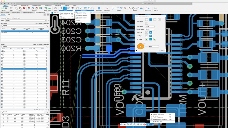
Features such as interactive routing (US site), schematic capture and component libraries (US site) reduce design time. PCB design software also reduces the cost of production by optimising the placement of components, reducing the circuit board size and more.
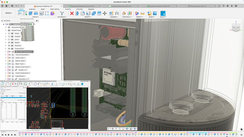
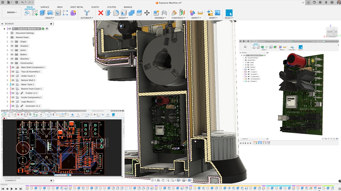
Fusion is a popular choice for PCB design thanks to its unique ECAD-MCAD integration, which synchronises electronic layouts with mechanical constraints in a single environment.
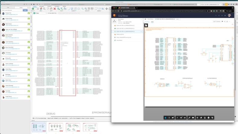
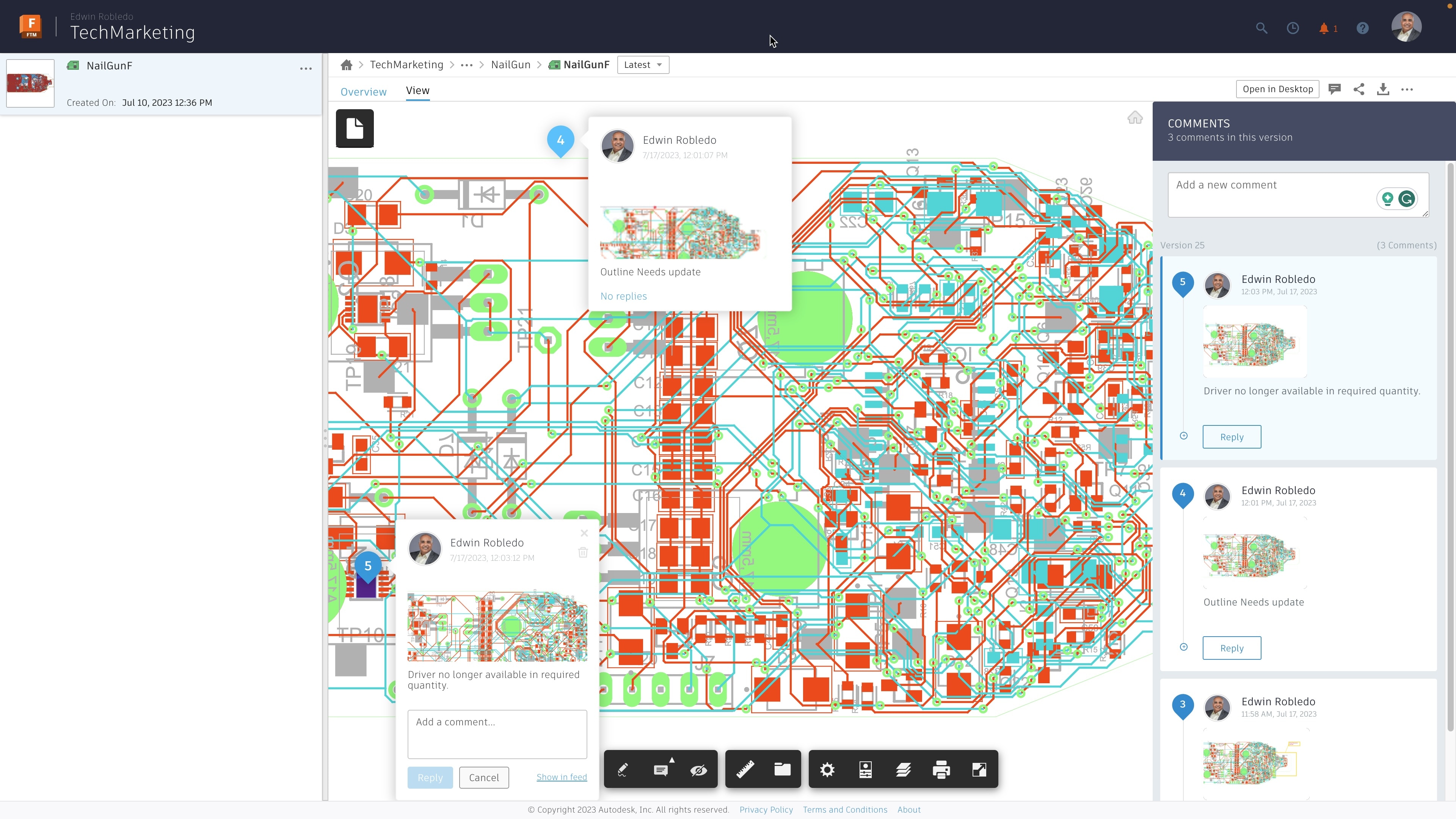
Cloud collaboration tools and built-in data management let design teams share work in real time with version control and instant feedback. Everything happens on one unified platform, making distributed teamwork simple and seamless.
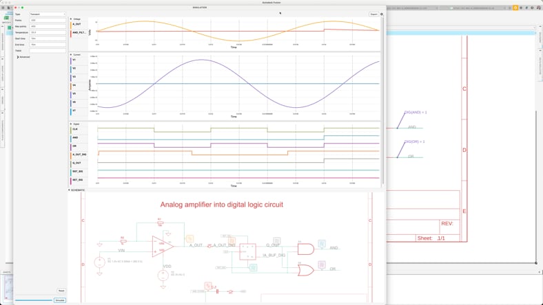
Fusion also simplifies PCB design with automatic checks, SPICE simulation and flexible rules so you can easily catch and fix mistakes before they go to manufacturing.
Here are some of the top PCB design features in Fusion:
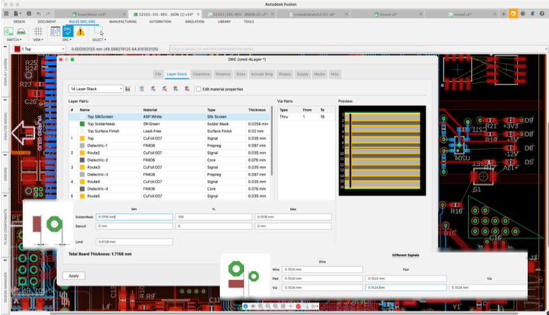
Uncover meticulous design guidelines, guaranteeing scalability and organisation for the most intricate PCB design constraint manager. Autodesk Fusion provides high-quality, error-free production through strict compliance with industry standards and optimisation of design specifications.
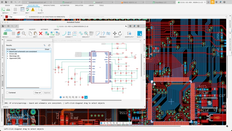
Fusion's PCB and schematic design synchronisation ensures confidence and minimises the risk of errors, enhancing the reliability of the final product. This integrated approach streamlines the design process, reducing the likelihood of discrepancies and ensuring consistent performance.
Verify that your design parameters are correct with our easy-to-use SPICE simulation tool, available in Fusion Electronics. Our repository of components makes it easy to get you started or build your own. It is SPICE compatible.
The Fusion electronics design capabilities provide managed team access to the project with instant updates to the latest version. Built-in versioning, milestone referencing and web-based access to designs enable stakeholders to comment, track progress and collaborate effectively.
PCB design follows a clear workflow, from schematic design to PCB layout, validation and manufacturing – and Autodesk Fusion connects each step in a single, integrated environment.
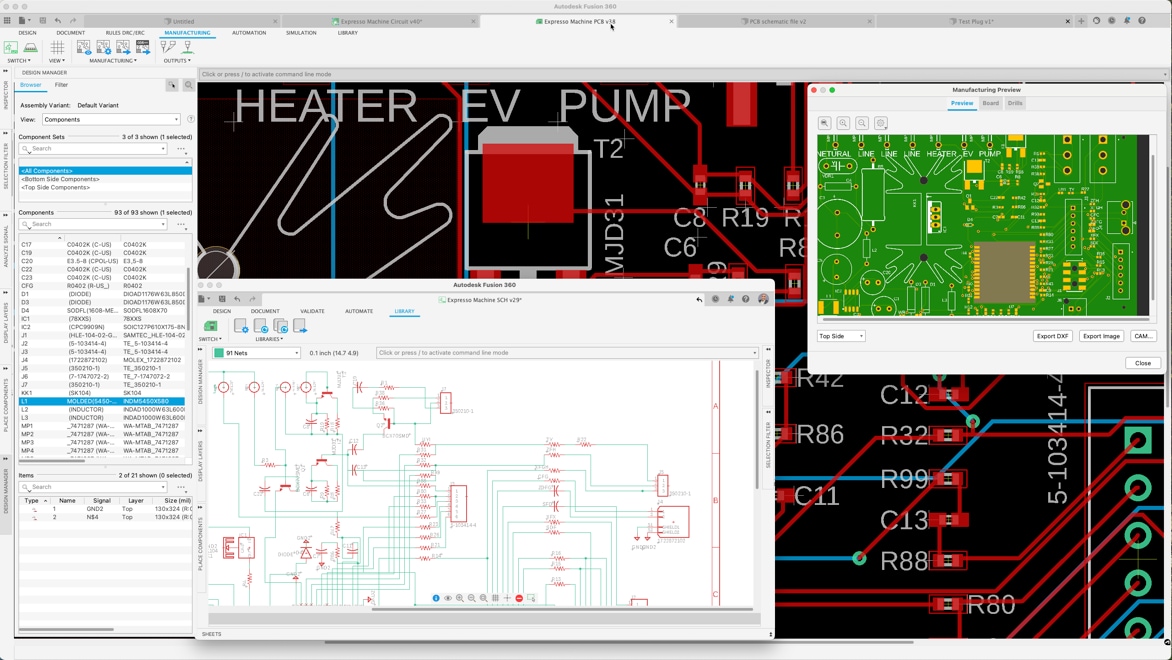
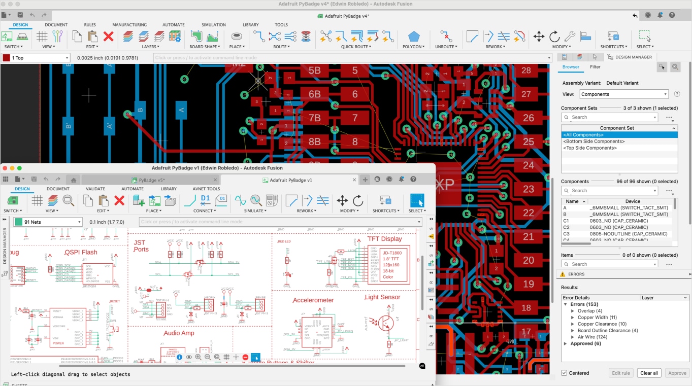
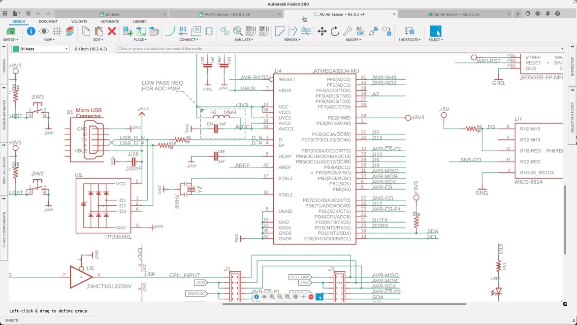
PCB design begins with schematic capture, where engineers define components, connections and electrical intent. In Autodesk Fusion, schematics are directly connected to the PCB layout, making sure design intent stays synchronised throughout the workflow.
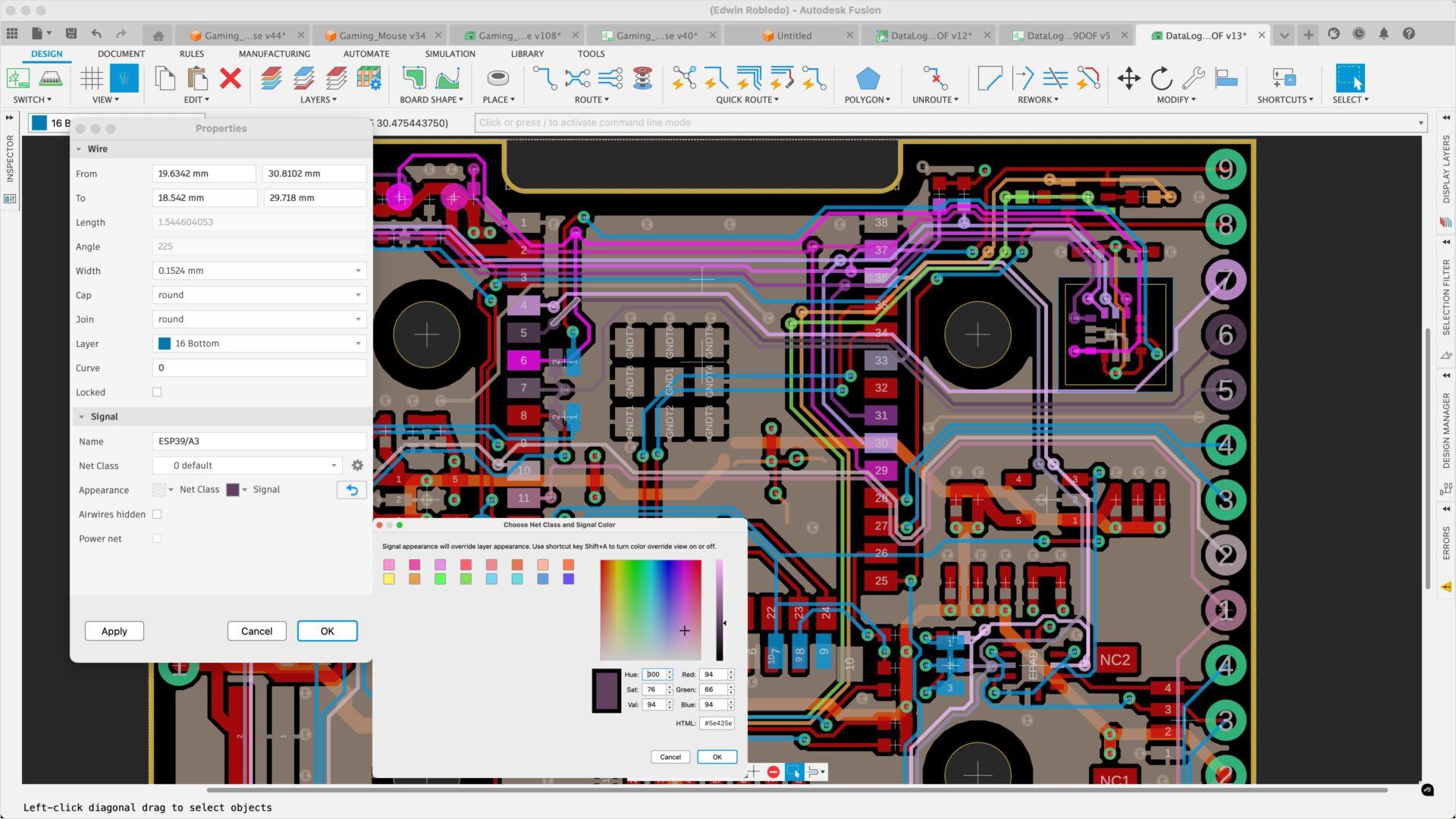
The schematic is translated into PCB board design by defining the board outline, placing components and routing copper traces. Fusion allows PCB layouts to be created in context of the mechanical enclosure, enabling early fit validation, connector alignment and clearance checks.
Design validation happens as the board is routed. Engineers can verify electrical rules, mechanical fit and thermal constraints while iterating on the layout. Fusion’s integrated ECAD–MCAD environment helps identify issues early, reducing late-stage design changes.
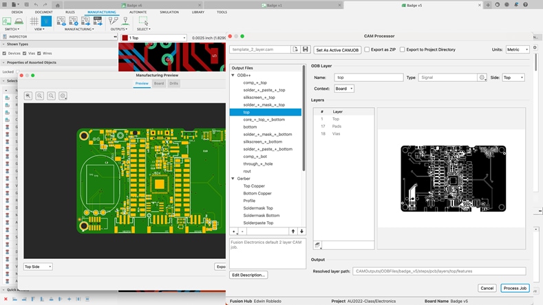
Once validated, PCB designs are prepared for manufacturing with accurate, up‑to‑date data. Because electrical, mechanical and design changes are managed in Autodesk Fusion, the handoff to manufacturing is smoother, with fewer errors and fewer revision cycles.
To design and optimise a PCB in Fusion, begin by launching the software and opening the electronic design workspace. Start with creating a detailed schematic using the extensive component libraries, then place components and connect them on your board layout.
Use the unified ECAD/MCAD environment to reduce rework and improve layout efficiency.
Validate your design before manufacturing by using SPICE simulation and signal integrity tools.
Autodesk Fusion integrates PCB design and mechanical design (US site) in a single environment, allowing engineers to validate enclosure constraints, board fit and component clearances early in the PCB board design process. PCB layouts are created directly in the context of the product enclosure, making it easier to confirm connector alignment, mounting locations and overall fit before prototypes are built.
This unified ECAD–MCAD workflow also helps teams address thermal constraints and manufacturing handoff earlier. Designers can assess component placement, airflow considerations and heat‑sensitive areas while routing the board, rather than discovering issues late in validation. By validating electrical, mechanical and thermal requirements together, Fusion reduces rework, streamlines collaboration and delivers PCB designs that are ready for manufacturing with fewer iterations.
Design for manufacturing (DFM) is the practise of creating PCB designs that can be reliably fabricated, assembled and tested at scale. Effective DFM considers manufacturing constraints such as trace widths, spacing, component placement, tolerances and board geometry early in the PCB design process, rather than treating manufacturing as a final step.
In Autodesk Fusion, PCB design, mechanical design and validation are connected, making it easier to align PCB board designs with manufacturing requirements from the start. By validating fit, mechanical constraints and design rules before handoff, teams can reduce errors, streamline collaboration with manufacturing partners and deliver PCB designs that move to production with fewer revisions.
Many PCB design issues are not electrical errors – they are workflow gaps that surface late in validation or manufacturing. Common mistakes include designing PCB layouts without full enclosure context, overlooking component height and connector alignment and addressing thermal constraints too late in the process. These issues often lead to fit problems, overheating and costly board revisions after prototypes are built.
Other frequent PCB design mistakes include overcrowded component placement, incomplete design rule checks and poor coordination between electrical and mechanical teams. When PCB design, enclosure design and manufacturing requirements are handled in separate tools, critical constraints can be missed. Using an integrated platform like Autodesk Fusion helps teams identify fit, clearance and thermal issues earlier, reducing rework and improving overall design reliability.
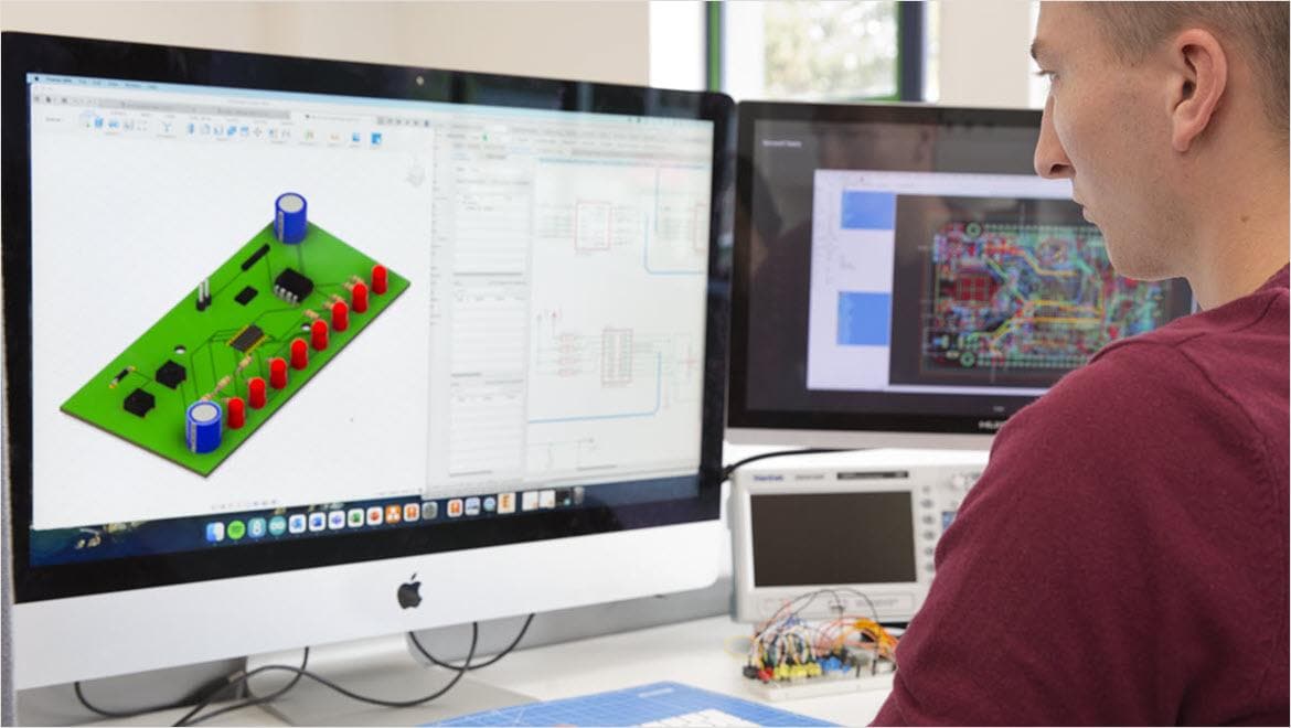
Schematic capture is what you do when you take a PCB design from your head or from notes and turn into a schematic diagram using PCB designing software. It’s not just about showing all the parts of a circuit. The diagram also needs to include the connections between them, which are often called “nets” in electronics CAD. Circuit board design software such as Fusion simplifies this process and helps you track everything.
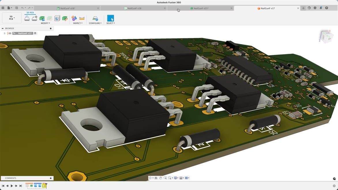
Circuit diagrams may be two-dimensional, but circuit boards are definitely not. Autodesk Fusion allows you to preview your PCB designs in 3D from the angle you choose, so you can take a look at it from a whole new perspective. This helps you better visualise how different components will interact and how the design will fit inside its casing. That way, you can avoid building costly, time-consuming prototypes only to start over if something doesn’t work.
Effective PCB design depends not just on connecting components and circuits but on connections between minds and an approval hierarchy. With Fusion, you can quickly and easily share your designs with colleagues and peers for feedback and guidance, review colleagues' work or get inspired by others’ PCB designs. You can even work on PCB cad designs with others simultaneously, speeding up design time and allowing you to benefit from having additional brain power on the task.
PCB design (US site) is the process of turning an electronic schematic into a physical printed circuit board by defining component placement, copper routing, layers and manufacturing constraints.
PCB design software, such as Autodesk Fusion, helps engineers create schematics, design PCB layouts, validate electrical and mechanical constraints and prepare files for manufacturing and assembly.
PCB design covers the full electronic workflow, including schematics and rules, while PCB board design (US site) focuses on the physical layout of the board, such as placement, routing and layers.
The PCB design workflow typically includes schematic design (US site), PCB layout, validation and manufacturing handoff.
Enclosure design affects board shape, component height, connector placement and clearances, making it critical to validate PCB fit early in the design process.
Component placement, copper routing and airflow all influence heat dissipation, making thermal considerations an essential part of PCB board design.
Before manufacturing, PCB designs should be validated for electrical rules, mechanical fit, thermal constraints and manufacturability (US site) requirements.
Yes. Fusion supports collaboration across electrical, mechanical and manufacturing teams by keeping PCB design data connected and up to date.
Autodesk Fusion connects schematic design, PCB board layout, mechanical context, validation and manufacturing handoff in a single platform.
Yes. PCB design software solutions, such as Autodesk Fusion allow PCB design and mechanical design to be performed in the same environment, keeping designs synchronised.
ECAD MCAD integration connects PCB layouts with mechanical design, enabling early fit validation, enclosure checks and improved collaboration between teams.
DFM (US site) reduces production errors, minimises costly redesigns and helps ensure PCB designs move smoothly from design to manufacturing.
Design for manufacturing (DFM) (US site) ensures that a PCB design can be reliably fabricated, assembled and tested by accounting for manufacturing constraints during layout.
PCB design mistakes can be reduced by validating electrical, mechanical and thermal constraints early and keeping design data connected across teams. Electronics simulation (US site) tools like those in Autodesk Fusion can help.
Common PCB design mistakes include poor component placement, ignoring enclosure constraints, addressing thermal issues too late and insufficient manufacturing validation. Try Autodesk Fusion free for 30-days (US site) to take your PCB designs to the next level.