 Sam Sattel
3D PCB design software such as Autodesk Fusion creates an environment for designers to coexist in the worlds of ECAD and MCAD.

Elevate your design and manufacturing processes with Autodesk Fusion
Most printed circuit board (PCB) designers are familiar with utilizing different software for a singular project. Differing PCB software can hinder efficient 3D electronic design, manifest miscommunication, and stall functionality. Let’s explore the three main benefits of using PCB design software to combine ECAD (electronic computer-aided design) and MCAD (mechanical computer-aided design): bidirectional workflows, cloud-based data management, and single-sourced library.
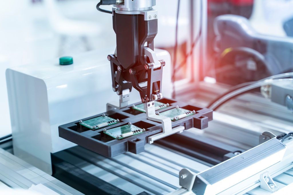
3D printed circuit board design
The old method of testing board-to-board and component-to-component interference was executed using third-party software that required manual comparisons. However, 3D PCB software such as Fusion creates a single environment for designers to coexist in the worlds of ECAD and MCAD. PCB design begins with a foundation of schematic creation, library management, and PCB layout. You can learn more about this process through our recent collaboration with tutorial resource TeachmePCB.com.
Traditional PCB design
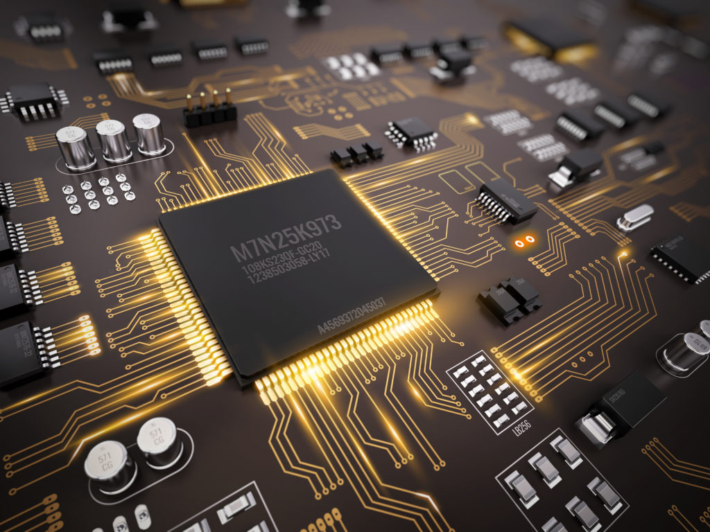
PCB software that does not integrate more than a couple of PCB design components is essentially outdated for the needs of current electronics designers. Traditionally, MCAD and ECAD worked independently and did not always communicate or transfer 2D or 3D models correctly.
How do MCAD and ECAD work?
MCAD is ideal for various design iterations (form factors and physical placements) and provides a 3D visual reference for testing structural integrity. MCAD combines CAD, CAM, and CAE; however, when MCAD is not integrated with ECAD, the user must manually check the 3D design to ensure that board components do not interfere with each other.
ECAD is a software workflow based on electronics design. ECAD programs usually include component libraries, layout editors, and schematic editors. ECAD software allows for experimentation with multiple or stacked PCB boards, tests thermal performance, and ensures PCBs comply with defined requirements.
After initial designs are transferred between MCAD and ECAD software and requirements are met, a prototype is created. As described, this transfer process is robust. It generates an increased risk of data transfer errors and human communication errors, which can be minimized when MCAD and ECAD are integrated into a collaborative PCB software.
MCAD/ECAD collaboration

Using two separate software environments to create one cohesive prototype can be frustrating and time-consuming. PCB design software collaboration optimizes PCB assembly and reduces the risk of error. MCAD and ECAD integration allow for a one-stop-shop of accuracy.
Bidirectional workflows
Bidirectional workflow routing promotes collaboration and flexibility during the design and prototyping processes. The modern design process has evolved beyond singular workflows and instead reaches for a coherent and forgiving system. Streamlined bidirectional workflows allow engineers to fix mistakes or make last-minute changes without sacrificing large segments of time.
Cloud-based data management
Cloud-based data management provides a unique setting where MCAD and ECAD collaboration is routed and communicated in real-time. Cloud-based solutions avoid traditional errors incurred by divided MCAD and ECAD PCB design software. Multiple users can work on the same board layout without missing any revisions, and designs can easily be shared with PCB manufacturers to be turned into real electronic products.
Single sourced library
A cloud-based library of PCB schematic symbols, 2D footprints, and 3D models sew workflows and data management together to create instant comparisons of 3D PCB design.
Try Fusion’s integrated MCAD/ECAD PCB design platform to experience team access to a common design environment with a dedicated management system suitable for the most intricate 3D printed circuit board and electronic component designs.
Frequently asked questions
PCB design directly impacts product reliability because board layout influences electrical performance, thermal behavior, manufacturability, and long-term durability. Poor component placement, inadequate trace routing, thermal hotspots, and insufficient clearances can lead to signal integrity issues, overheating, premature component failure, and increased defect rates in production. Proper PCB design helps ensure consistent performance throughout a product’s lifecycle.
Autodesk Fusion supports reliable PCB development through schematic capture, design rule checking (DRC), 3D PCB visualization, ECAD-MCAD integration, and simulation tools that help identify potential issues before manufacturing.
Design for Manufacturability (DFM) helps ensure a PCB can be produced efficiently, consistently, and cost-effectively. A design may function correctly in theory but still be difficult or expensive to manufacture if component spacing, routing, soldering requirements, or assembly constraints are overlooked. DFM reduces production defects, minimizes rework, improves yield, and helps shorten the time between design completion and production.
Autodesk Fusion supports DFM through design rule checks, PCB manufacturing outputs, component validation, 3D visualization, and integrated workflows that connect design decisions directly to manufacturing requirements.
Design errors often appear as assembly failures, soldering defects, electrical shorts, open circuits, thermal problems, electromagnetic interference (EMI), or components that do not fit correctly within the product enclosure. In many cases, these problems are not discovered until prototypes are assembled or tested, increasing development costs and delays.
Autodesk Fusion helps reduce these risks by keeping PCB and mechanical designs synchronized, validating designs with design rule checks, and allowing engineers to review board layouts in a realistic 3D environment before release.
PCB design mistakes can be avoided through early validation, consistent design rules, cross-functional collaboration, and manufacturability reviews throughout development. Engineers should verify schematics, perform design rule checks, evaluate thermal performance, confirm mechanical fit, and review manufacturing outputs before release.
Autodesk Fusion helps teams catch problems earlier by combining PCB design, mechanical design, visualization, simulation, and manufacturing preparation in a single platform. Because electronics and mechanical teams work from connected data, design changes can be evaluated before they become costly production issues.
Simulation allows engineers to evaluate PCB performance before building physical prototypes. By analyzing thermal behavior, cooling effectiveness, and real-world operating conditions, simulation helps identify overheating risks, reliability concerns, and potential performance bottlenecks early in development.
Autodesk Fusion includes simulation capabilities that help teams validate designs, evaluate PCB assemblies, and analyze electronics cooling performance before manufacturing. This can reduce design iterations, lower prototyping costs, and improve confidence in final design decisions
A PCB design is typically ready for manufacturing when it has passed design rule checks, been verified for electrical and mechanical requirements, validated for manufacturability and assembly, and includes all required production outputs such as Gerber files, bills of materials (BOMs), and assembly documentation. Manufacturing-ready designs should also account for thermal management, component availability, and assembly constraints.
Autodesk Fusion helps streamline this process by keeping schematics, PCB layouts, 3D models, and manufacturing outputs connected within a single workflow, reducing the risk of errors during handoff to production.
Design for manufacturing (DFM) catches problems before a board goes to fabrication, not after. In Fusion, DFM checks run against the same design rules the fabricator uses: trace width and spacing, drill sizes, annular ring, and copper-to-edge clearance. Because the check happens inside the same environment as layout, a designer can fix a violation immediately instead of discovering it in a fabrication rejection days later. Skipping DFM review is one of the most common reasons a board comes back from the fabricator needing a respin.
A board’s reliability is set largely at the design stage, not during assembly. Trace width has to carry the expected current without excessive heating, via placement affects how well heat and mechanical stress are managed, and copper pour design affects both thermal performance and signal return paths. In Fusion, designers can check these factors against the mechanical enclosure in the same model, so a board that passes electrical review does not later fail because it does not fit or vent heat properly inside its housing.
Most manufacturing failures trace back to a small set of design issues: insufficient clearance between traces or pads, missing solder mask openings, incorrect drill sizes, or footprints that do not match the actual component package. These show up as opens, shorts, or components that will not seat correctly during assembly. DRC (design rule check) in Fusion flags most of these before the design ever leaves the layout tool, comparing the board against fabrication and assembly rules rather than relying on manual inspection.
The most reliable way to avoid PCB design mistakes is to check the design against manufacturing constraints continuously, not just at the end. In Fusion, DRC runs against fabrication rules, assembly rules, and test requirements while the board is still being laid out, so violations get fixed at the point they are introduced. Combining that with a 3D check against the mechanical enclosure catches the other common category of late-stage failure: components or connectors that clash with the housing.
Simulation lets a designer verify a decision before committing to fabrication. In Fusion, that includes checking things like copper pour effectiveness and thermal behavior within the same workspace used for layout, so a designer does not have to export the board to a separate tool to get a basic read on whether a design choice will hold up. This shortens the iteration loop between making a change and knowing whether it worked.
A design is manufacturing-ready when it has passed DRC against the fabricator’s rules, generated complete Gerber and drill files, and been checked against the mechanical enclosure for fit. Fusion produces the full fabrication and assembly output set (Gerbers, drill files, pick-and-place, and BOM) from the same design used for layout, so there is no translation step between “the design looks right” and “the design is ready to send out.”