Take an in-depth look at PCB design and see how Fusion is a great solution for designing high-quality and high-performance PCBs.
Printed circuit boards (PCBs) are the backbone of modern electronic devices. They provide the physical and electrical foundation required for the functioning of everything from smartphones to appliances to industrial machinery. This comprehensive article will delve into the details around PCBs and why Autodesk Fusion is a good solution for PCB design.
What is a PCB?
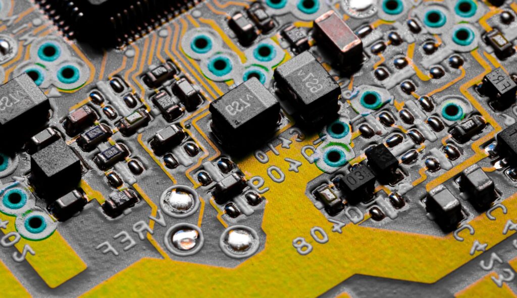
A Printed circuit board (PCB) is a flat, typically rectangular piece of non-conductive material that hosts electrical components connected by conductive pathways. These pathways, or traces, are etched onto the board, allowing electrical signals to flow between components such as resistors, capacitors, and integrated circuits. PCBs offer a compact, reliable, and cost-effective method of assembling electronic components into a functional circuit. They come in various forms, including single-sided, double-sided, and multi-layered boards, each with unique applications and advantages.
Elevate your design and manufacturing processes with Autodesk Fusion
The term “PCB board” is often used interchangeably with PCB, but it specifically refers to the physical board itself, excluding the components. The PCB board provides the foundation for mounting and interconnecting electronic components. It typically includes the cross-section of the PCBs, each contributing to the board’s overall functionality.
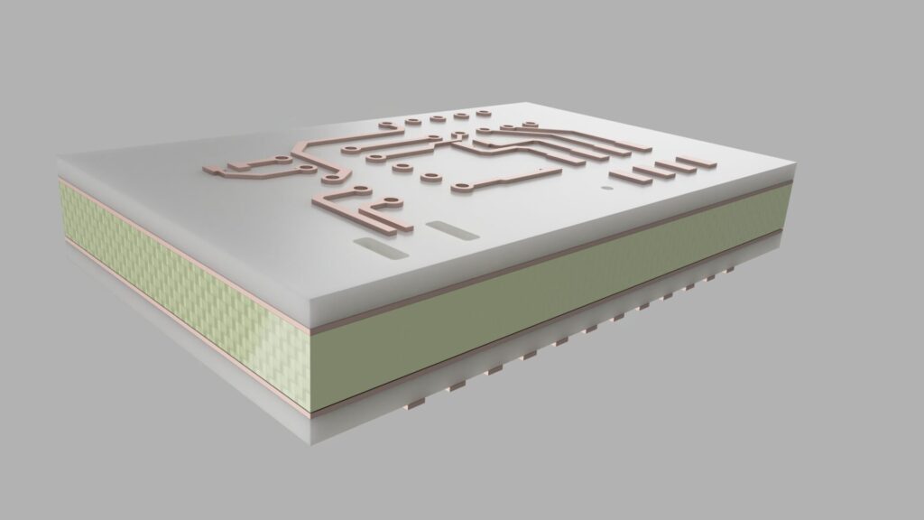
Cross-sections of a PCB
A PCB includes multiple layers, each serving a specific purpose. Here are the primary layers in a typical multi-layer PCB:
1. Substrate/Core: This is the base material of the PCB that provides structural support and insulation for the board. They are typically made of fiberglass-reinforced epoxy resin.
2. Copper layer: These layers are thin sheets of copper laminated onto the substrate that form the conductive pathways that connect the components. Multi-layer PCBs have several copper layers for complex circuitry.
3. Solder mask: These are a protective layer applied over the copper traces to prevent short circuits and oxidation. Ot times, there are green, giving PCBs their characteristic green color, although other colors are available.
4. Silkscreen: This layer contains printed information such as component labels, logos, and other markings to assist in assembly and troubleshooting.
5. Adhesive/Prepreg: In multi-layer PCBs, Prepreg is a fiberglass material pre-impregnated with resin, used to bind the layers.
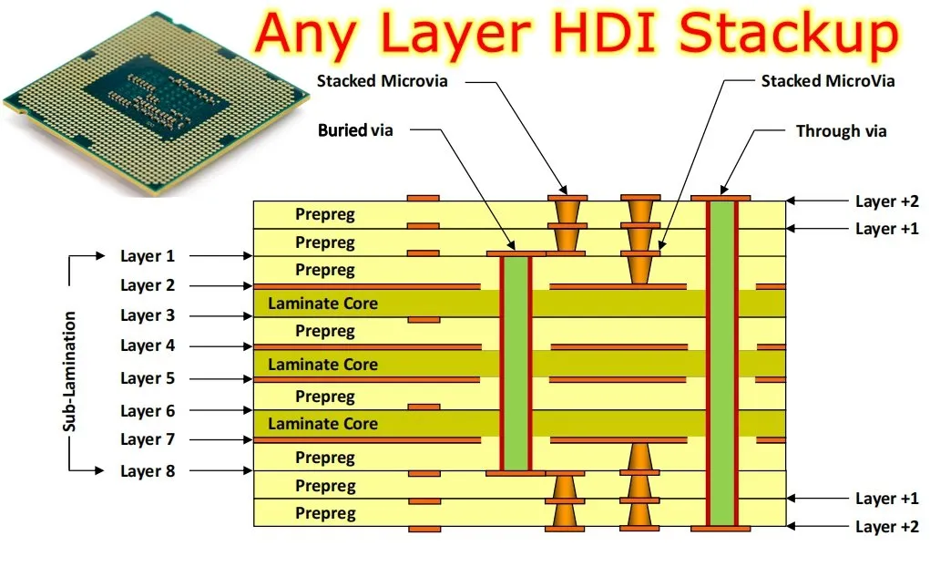
What are HDI PCBs?
High-density interconnect (HDI) PCBs contain a higher density of wiring compared to traditional PCBs. HDI technology allows for faster signal transmission, improved reliability, and better utilization of space, contributing to the ongoing miniaturization and sophistication of electronic devices. The boards have finer lines and spaces, smaller vias, and higher connection pad density, allowing for more components to in a smaller area. HDI PCBs commonly use advanced technologies such as microvias, buried vias, and blind vias to achieve this increased density. These features assist in the creation of complex and compact electronic devices with enhanced performance. HDI PCBs are ideal for smartphones, tablets, and other high-performance consumer electronics.
PCB design
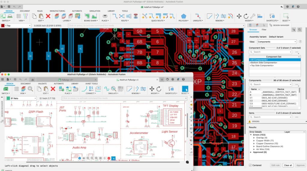
PCB design is the process of creating the layout and arrangement of components and traces on a printed circuit board (PCB). It includes various steps, starting with schematic design. Here a diagram representing the electrical connections between components is created, serving as a blueprint for the PCB layout. Next, place components on the PCB to optimize space, performance, and manufacturability. During this step, it’s important to consider factors such as signal integrity, thermal management, and ease of assembly.
Next, perform a design rule check (DRC) to make sure that the design adheres to manufacturing and electrical standards. At this point, its important to check for issues such as trace width, spacing, and clearance. Next comes routing. Here, traces are drawn to connect the components according to the schematic. It’s important to make sure that traces do not overlap or create short circuits; this can be done manually or automatically using CAD software. Finally, Gerber files are generated, containing the information needed for manufacturing the PCB, including the copper layers, solder mask, and silkscreen.
PCB assembly
The PCB assembly process involves mounting and soldering electronic components onto the PCB board. This process can be done manually for small-scale production or for large-scale manufacturing using automated machinery. The primary steps in PCB assembly include solder paste application, where solder paste is applied to the PCB pads to secure components during soldering. Next, components are placed onto the PCB. This can be done manually or using pick-and-place machines. The PCB then passes through a reflow oven or wave soldering machine to melt the solder paste. This creates a permanent connection between the components and the PCB. Last, the assembled PCB undergoes inspection and testing to ensure proper functionality. Typically, techniques such as X-ray inspection and automated optical inspection (AOI) detect defects.
Key considerations during PCB assembly
During PCB assembly, it’s important to optimize the design formanufacturability (DFM) by making sure the layout is conducive to easy, cost-effective production. Proper component placement is necessary assembly and to reduce errors, considering both thermal and electrical performance. The choice of soldering method, such as wave or reflow soldering, should align with the components and design specifics, maintaining appropriate soldering temperatures to avoid damage. Quality control measures, including automated optical inspection (AOI) and X-ray inspection, are necessary for detecting defects early. Selecting high-quality materials for the PCB substrate and components ensures durability and effective thermal management. Techniques like heat sinks, thermal vias, and strategic PCB layout help manage heat dissipation.
Further, managing electromagnetic interference (EMI) and ensuring signal integrity through proper grounding, shielding, and trace routing is of utmost importance. Sourcing components from reputable suppliers helps mitigate risks associated with quality and availability. The PCB assembly process should be compliant with industry standards and regulatory requirements, such as IPC standards and RoHS compliance to make sure that the PCB assembly meets necessary guidelines.
Types of PCB boards
PCBs come in various types, each designed for specific applications and requirements:
- Single-sided PCBs: Thes are simple and cost-effective, suitable for low-complexity circuits and include a single layer of copper on one side of the substrate.
- Double-sided PCBs: These have copper layers on both sides of the substrate, allowing for more complex circuitry. Vias (holes) connect traces on both sides.
- Multi-layer PCBs: They are used in high-density, high-performance applications such as smartphones and computers and consist of multiple layers of copper and substrate stacked together.
- Rigid PCBs: These provide structural support and are made from solid, inflexible materials and are found in most electronic devices.
- Flexible PCBs: These PCBs can bend and twist and are ideal for applications with limited space or moving parts.
- Rigid-flex PCBs: These are commonly used in medical devices and wearable technology and combine rigid and flexible sections.
- High-frequency PCBs: These use specialized materials to minimize signal loss and interference and are designed for high-frequency applications.
- High-density interconnect (HDI) PCBs: These use microvias, blind vias, and buried vias to achieve compact designs and have a higher density of interconnections as compared to standard PCBs.
Industry applications of PCBs
PCBs are in virtually every industry that relies on electronic devices. Some common applications include:
- Consumer electronics: Smartphones, tablets, laptops, and appliances rely on PCBs for their functionality and compact design.
- Automotive: Vehicles use PCBs in infotainment systems, advanced driver-assistance systems, and engine control units.
- Aerospace: PCBs are using in avionics, navigation equipment, and communication systems.
- Medical devices: Diagnostic machines, monitoring devices, and implants use PCBs for precision.
- Renewable energy: Wind turbines, solar panels, and energy storage systems use PCBs for power management and conversion.

History of PCBs
The concept of printed circuit boards (PCBs) dates back to the early 20th century, with significant milestones marking their historical development. In 1903, German inventor Albert Hanson filed a patent for a method of creating flat, insulated conductors on a board, laying the groundwork for PCBs. During the 1920s, Charles Ducas advanced PCB technology by filing a patent for an electroplating method to create electrical paths on an insulated surface.
In 1943, the first true printed circuit board was developed by Austrian engineer Paul Eisler while working on a radio set in the UK. His design utilized etched copper foil on a non-conductive substrate. The 1950s brought widespread adoption of PCBs in consumer electronics and military applications. In the 1960s integrated circuits (ICs) and multi-layer PCBs were introduced, allowing for the creation of more compact and powerful devices.
The emergence of surface-mount technology (SMT) in the 1980s allowed components to be mounted directly on the PCB surface, further reducing size and increasing complexity. In the 2000s, HDI PCBs and advanced materials facilitated the development of even smaller, faster, and more reliable electronic devices.
Autodesk Fusion for PCB design
Autodesk Fusion is a versatile and powerful integrated product development solution that offers comprehensive tools for PCB design, offering numerous features for PCB design, including:
- Schematic capture: Create detailed schematics that define the electrical connections between components. Fusion 360 provides an intuitive interface for drawing and editing schematics.
- Component libraries: Access a vast library of components, including resistors, capacitors, ICs, and connectors to create custom components and manage libraries.
- Design constraint manager: Discover precise design guidelines that ensure scalability and organization for complex PCB constraint management.
- PCB and schematic design synchronization: Integrated synchronization streamlines the design process, reducing discrepancies and ensuring consistent performance.
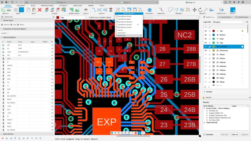
- Routing: Draw traces to connect components according to the schematic. Fusion offers both manual and automatic routing options to ensure efficient and reliable connections.
- Design rule check (DRC): Ensure designs adhere to manufacturing and electronics standards with DRC to check for issues such as trace width, spacing, and clearance.
- 3D PCB visualization: Examine the PCB in a realistic 3D environment, enabling you to analyze the design and spot potential issues. Fusion offers tools for rotating, zooming, and inspecting the 3D model in detail.
- Simulation and analysis: Evaluate the performance and reliability of the PCB design using simulation and analysis tools to identify and address potential issues before manufacturing.
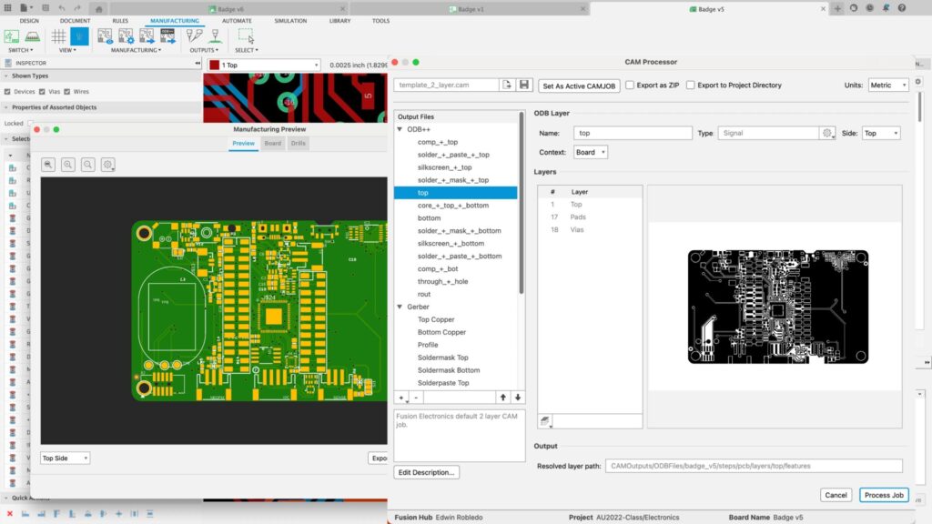
- Gerber file generation: Once the design is complete, generate Gerber files for manufacturing. Export the necessary files, including copper layers, solder mask, and silkscreen.
- SPICE simulation: Verify that your design parameters are correct with easy-to-use SPICE simulation.
- Collaboration: Built-in versioning, milestone referencing, and a cloud-based platform access enables stakeholders to comment, track progress, and collaborate effectively

Expand PCB design with the Autodesk Fusion Signal Integrity Extension
The Autodesk Fusion Signal Integrity Extension integrates powerful signal analysis tools directly into your PCB design workflow, leveraging Ansys technology to:
- Identify and resolve signal issues early.
- Meet EMC and EMI standards.
- Analyze trace coupling effects.
- Reduce prototype costs.
- Enhance product reliability.
Benefits
Improve high-speed PCB design compliance with EMI and EMC standards using Autodesk Fusion’s signal integrity tools.
Accelerate your development cycle by virtualizing electromagnetic analysis and simulation early in the PCB design process, improving your product development workflow.
Lower physical testing costs by minimizing expensive PCB prototyping and board re-spins with insights into your design’s electromagnetic signal performance.
How to start a new PCB design in Autodesk Fusion
Starting a new PCB design in Autodesk Fusion 360 is a straightforward process. Here’s how to start:
- Create a new project: Open Fusion and create a new project to serve as the workspace for your PCB design.
- Schematic capture: Use the schematic capture tool to draw and connect components. Next, define the electrical connections and ensure that the schematic is complete.
- Component placement: Once the schematic is complete, switch to the PCB layout view. Place components on the PCB, optimizing space and performance.
- Routing: Draw traces to connect the components according to the schematic and use routing options for confirm reliable connections. Perform a DRC to check for any issues.
- 3D visualization: View the PCB in 3D to analyze the design and identify issues. Rotate, zoom, and inspect the 3D model to ensure that it meets design specifications.
- Simulation: Evaluate the performance and reliability of the PCB design using simulation and analysis tools to address any issues identified during the simulation.
- Generate Gerber files: Once the design is complete, generate Gerber files for manufacturing the PCB.
- Collaboration: Share the design with stakeholders for review and feedback and to make necessary adjustments.
Printed circuit boards (PCBs) are fundamental to modern electronics, providing the foundation for assembling and interconnecting electronic components. Understanding the cross-sections, types, design processes, and assembly of PCBs is crucial for creating reliable and high-performance electronic devices. Fusion offers a comprehensive and integrated platform for PCB design to create sophisticated PCB designs that meet the highest standards of quality and performance. Start your PCB journey with Fusion today.
FAQ: PCB design software for modern product development
PCB design software integrates with mechanical design by enabling ECAD‑MCAD collaboration, where electronic and mechanical teams work from a shared, synchronized model.
Autodesk Fusion generates a 3D PCB (solid BRep) directly from the schematic and board layout, which acts as the live interface between electronics and mechanical design. When the PCB changes, those updates can be reflected in the mechanical assembly, helping teams identify fit, clearance, and interference issues early in the design process.
PCB software supports version control by tracking design revisions, history, and updates across schematics, board layouts, and 3D representations.
Autodesk Fusion uses cloud‑based data management to keep electronic and mechanical designs in sync. Version history ensures teams are working from the latest approved design, while controlled updates reduce errors caused by outdated files or disconnected ECAD and MCAD data.
Core features of PCB design software typically include:
-Schematic capture and PCB layout
-Component libraries and custom part creation
–Design rule checking (DRC)
-3D PCB visualization
-Manufacturing outputs for fabrication and assembly
Autodesk Fusion includes these core capabilities while also integrating PCB design directly with mechanical design, simulation, and manufacturing workflows—reducing the need for separate tools and manual handoffs.
When choosing PCB design software, key factors to consider include:
-Integration with mechanical design tools
-Ease of collaboration and version control
-Component library quality and reuse
-Manufacturing documentation and outputs
-Ability to scale as products become more complex
Autodesk Fusion is designed for teams that need PCB design as part of a broader product development workflow, combining electronics, mechanical design, and data management in one cloud‑connected platform
PCB design is the end‑to‑end process of creating electronic circuits, including schematic design, component selection, and electrical connectivity.
PCB board design focuses specifically on the physical layout of the board, including trace routing, layer stack‑up, and component placement.
In Autodesk Fusion, schematic design and PCB board layout are directly connected, ensuring that electrical intent and physical implementation stay aligned throughout the design process.