Avoid PCB respins by validating schematics, DFM, mechanical fit, and manufacturing data before release using connected workflows in Autodesk Fusion.
Elevate your design and manufacturing processes with Autodesk Fusion
Sending a PCB to manufacturing is one of the most expensive moments in product development. Mistakes discovered after this point multiply quickly. A missed clearance, a mismatched footprint, or an overlooked mechanical constraint can trigger respins, delays, and avoidable cost.
The teams that ship reliably don’t rely on last‑minute checks. They validate deliberately, across electrical intent, physical reality, and manufacturing constraints, before files ever leave the design environment.
1. Schematic and layout must match exactly
Before worrying about manufacturability, the design itself must be internally consistent. That starts with validating that the schematic, layout, and bill of materials are fully aligned.
Common failure points include:
- Netlist mismatches between schematic and PCB layout
- Incorrect or outdated footprints
- Component orientation or polarity errors
These issues are among the most common causes of non‑functional boards and are typically preventable with disciplined validation early in the workflow.
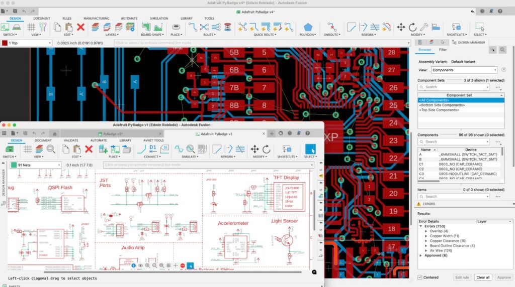
In Autodesk Fusion, schematic capture and PCB layout live in a connected environment, helping teams keep electrical intent and physical implementation synchronized as designs evolve.
2. Design for manufacturability (DFM) is not optional
Passing basic design rule checks isn’t the same as being manufacturable. DFM validation ensures the board can actually be built, realiably and at scale using real fabrication and assembly processes.
Critical DFM areas to validate include:
- Trace width and spacing against fab capabilities
- Drill sizes, aspect ratios, and annular rings
- Solder mask openings and silkscreen clarity
- Fiducials, panelization, and tooling features
Industry checklists consistently show that DFM oversights are a leading cause of fabrication holds and respins.
Fusion supports DFM‑aware design by allowing teams to validate rules continuously during layout, rather than discovering issues only at file export.
3. Mechanical fit must be proven, not assumed
Many PCB issues don’t originate in electronics at all. They show up when a board doesn’t fit its enclosure, a connector collides with a housing, or component heights exceed mechanical limits.
Validating mechanical integration before manufacturing means confirming:
- Board outline and mounting holes align with the enclosure
- Component heights meet clearance requirements
- Connectors, buttons, and displays align correctly
Fusion’s ECAD‑MCAD integration enables teams to validate PCB designs directly in a 3D mechanical context, reducing late‑stage surprises caused by disconnected tools.
4. Manufacturing outputs must be complete and unambiguous
Even a perfect design can fail if manufacturing data is incomplete or unclear. Before release, teams should validate that all outputs are accurate, complete, and aligned with the manufacturer’s expectations.
This includes:
- Gerber or ODB++ files
- Drill and stackup information
- Assembly drawings and pick‑and‑place data
- Bill of materials with approved components
Incomplete or inconsistent outputs are a frequent cause of production delays, even when the PCB layout itself is sound.
5. Validation is a process, not a final step
The most reliable teams don’t treat validation as a single gate at the end of design. They build it into the workflow, validating continuously as decisions are made.
Autodesk Fusion supports this approach by keeping electronics, mechanical design, and manufacturing preparation connected in one environment. This helps teams catch issues when they’re cheapest to fix.
Sending a PCB to manufacturing is not just a handoff, it’s a commitment. Validating schematic integrity, manufacturability, mechanical fit, and manufacturing data before that moment dramatically reduces risk, cost, and time‑to‑market.
The goal isn’t perfection. It’s confidence.
And confidence comes from validation that’s done early, done thoroughly, and done in context.
FAQ: PCB design and manufacturing readiness
PCB design is important because it directly affects a product’s functionality, reliability, manufacturability, and cost. The printed circuit board forms the physical foundation that connects and supports electronic components, so errors at the PCB design stage can lead to performance issues, manufacturing defects, or complete product failure.
Modern PCB design tools like Autodesk Fusion help teams validate electrical intent, physical layout, and mechanical fit early, reducing the risk of downstream issues during assembly and production.
PCB design software solves the complexity of translating electronic schematics into manufacturable, reliable circuit boards. It helps teams manage component placement, routing, spacing, and electrical rules while preparing outputs for fabrication and assembly.
With integrated platforms such as Autodesk Fusion, PCB design software also enables 3D visualization, design rule checks (DRC), and electronics‑to‑mechanical collaboration, reducing errors caused by manual layout, disconnected tools, or late‑stage design changes.
The biggest risks in PCB design include signal integrity issues, thermal problems, manufacturability errors, and poor cross‑discipline coordination. Inadequate spacing, incorrect routing, or overlooked manufacturing constraints can lead to board re‑spins, compliance failures, or reliability issues in the field.
It’s recommended to address these risks early through integrated DRC, simulation, and design‑for‑manufacturing checks before fabrication begins to avoid costly delays and redesigns.
Design for Manufacturing (DFM) is important for PCB design because it ensures that a board can be produced reliably, cost‑effectively, and at scale. Without DFM considerations, even electrically correct designs can fail during fabrication or assembly due to placement constraints, soldering issues, or material limitations.
PCB workflows in Autodesk Fusion support DFM by helping teams evaluate component placement, thermal behavior, spacing rules, and manufacturing constraints early in the design process, reducing board re‑spins and improving production outcomes.