Check out these steps for designing with the end goal of getting a working PCB prototype back from your manufacturer the first time.
We all want our PCB prototypes to get done as fast and as cheap as possible, but sometimes this just doesn’t happen. After all, when you start a new design and focus all of your time on your circuit design or component selection, then you have little time left over for your PCB layout. But in the world of PCB manufacturing, when it’s time to turn an idea into a board, then the layout process is what matters most.
Elevate your design and manufacturing processes with Autodesk Fusion
So what’s the key to designing a PCB that gets you a working prototype back right the first time? We’ve got our top 10 design decisions below to make it happen.
Table of Contents
- 1. Be mindful of your component placement
- 2. Define your trace widths before designing
- 3. Keep your electromagnetic interference in check
- 4. Orient your power and ground planes
- 5. Add accurate silkscreen marking
- 6. Avoid mixing leaded and lead-free components
- 7. Double Check For Solder Mask Between Pads
- 8. Leave Clearance Between Your Copper and Board Edge
- 9. Identify heating issues before they start
- 10. Double-check for acute angles on your traces
- Good boards, good times
1. Be mindful of your component placement
When placing components on your PCB layout, you always need to be thinking in the back of your mind how your parts will be soldered. Are you working with SMT components that need to run through a wave solder machine (edited)? Then you’ll want to orient all of your parts of a similar type in the same direction.
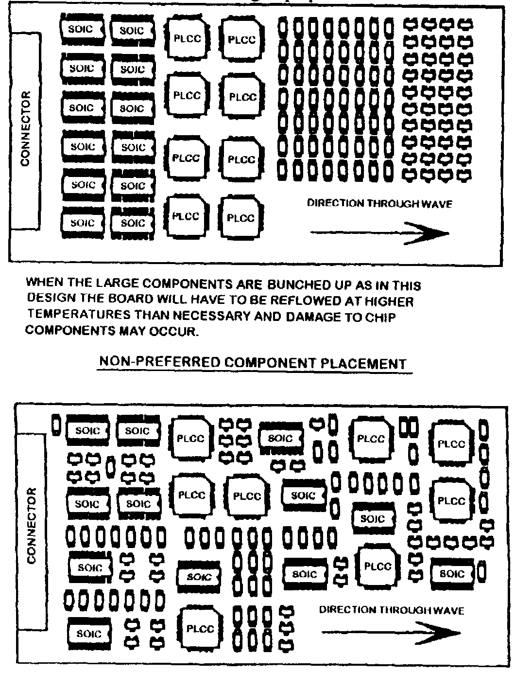
We also recommend placing all of your surface mount components on the same side of your board to avoid multiple spins through the soldering equipment (edited). And try keeping all of your through-hole parts on the top side of your board to minimize how many steps are required to assemble your parts by hand.
2. Define your trace widths before designing
Before you even begin laying down parts or routing nets, you need to know how wide your traces need to be to carry their required current. As a general guideline, we recommend having your traces set at 0.010” for low current analog and digital signals.
If you’re working with traces that will be pumping out more than 0.3 amps, then make your traces wider. And you don’t need to do all of these manual calculations by hand to determine trace widths. Just use a freely available trace width calculator as part of your pre-design prep work.
3. Keep your electromagnetic interference in check
We’ve all likely worked on circuit boards with large voltages and know that electromagnetic interference can mess up your low-voltage and current control circuits. To reduce the impact of interference, we recommend keeping your power ground and control ground planes separate for each power supply stage.
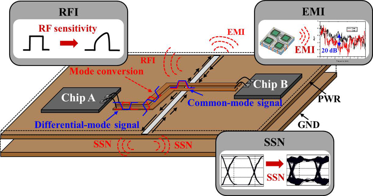
If you do happen to place your ground plane in the middle of your layer stackup, then also be sure to add an impedance path. This will reduce the chance of your power circuit interfering with other components on your board.
4. Orient your power and ground planes
We always recommend adding your power and ground planes in the internal layers of your board. The placement of these layers will help to keep your board more sturdy and ensure that it doesn’t bend during the component placement process. For Integrated Circuits (ICs), we also recommend using a common set of power rails that have wider trace widths to handle the increased heat that will be pouring through the copper.
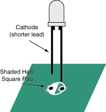
5. Add accurate silkscreen marking
We always recommend identifying components on your board in a simple and easy-to-understand manner that makes the component placement and orientation process as painless as possible. For example, adding helpful symbols that show where the anode and cathode ends of a diode are inserted will make your life a whole lot easier.
6. Avoid mixing leaded and lead-free components
There are a bunch of older components out there still in use that don’t have a lead-free option. While you might be tempted to toss one of these in with your newer lead-free parts, think again. Both lead and lead-free components have very different heat requirements, especially for RoHS-certified parts.
If you do need to mix lead and lead-free components, then consider putting something like a lead-free BGA on a leaded board, as opposed to a leaded chip on a lead-free board. The latter of these two scenarios will often lead to a board that overheats and evaporates all of its flux, creating an overly compressed and damaged PCB.
7. Double Check For Solder Mask Between Pads
It’s a common mistake to forget to add a solder mask layer between your pads. Maybe you pulled your design settings from a larger PCB over to a smaller one, and now you have pad holes that are too large. It happens.
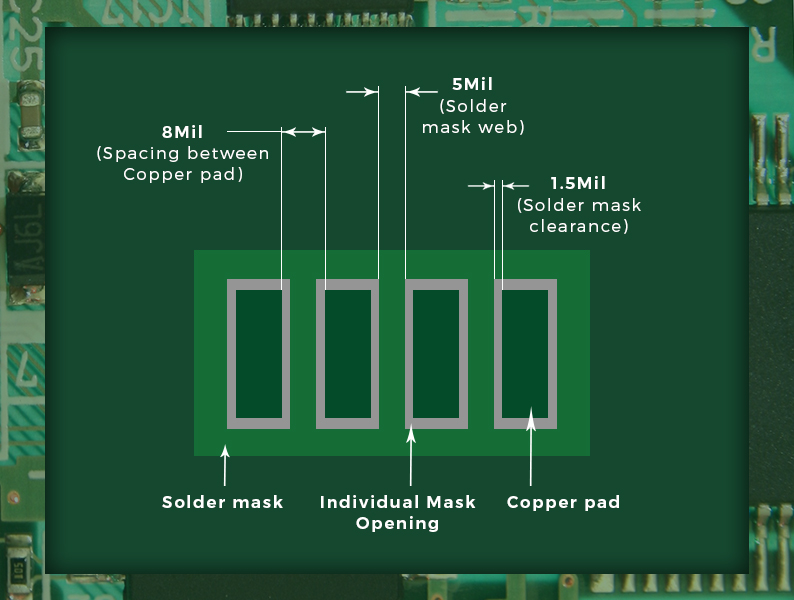
Whatever the reason, always double-check before sending your design off to your manufacturer that all of your pads have a layer of solder mask between them. This will help to fight against the risk of bridging and corrosion. When your design files do land in your manufacturer’s hands, they’ll also likely perform a complete DFM check to help spot any solder mask you might have missed.
8. Leave Clearance Between Your Copper and Board Edge
Whenever you design a PCB, we always recommend leaving a small amount of clearance between the edge of your board and any copper planes or traces. The last thing you want is for your PCB to get trimmed out of its panel during manufacturing and your copper to get trimmed as well. If this happens, the exposed copper will open your board to short circuits.
Set yourself up with some design rules in your DRC before you ever start your design process to define copper-to-edge or plate-to-edge clearances. If you keep a clearance of at least 50 mils, you should be safe. Always check with your manufacturer ahead of time to see what clearance requirements they recommend.
9. Identify heating issues before they start
If you’ve ever had the performance of a circuit degrade over time, then you know how costly heat issues can be in a manufactured product. To help keep your heating issues in check, always know what components on your board will pump out the most heat. You can find this information in any datasheet by looking for the Thermal Resistance ratings and their accompanying guidelines.
10. Double-check for acute angles on your traces
Most of us designers these days know to avoid making acute angles in our traces, but they can still slip through the cracks, especially when two traces join. During the PCB etching process, the presence of acute angles can lead to an acid buildup, which eats away at the copper and makes the circuit defective down the road.
When your routing process is complete, always review all of your traces, especially segments where two traces connect, for any acute angles. And during your routing process, opt for 45-degree trace angles instead of 90.
Good boards, good times
Want your PCB prototype back fast? Then, take the time to incorporate the 10 design decisions above in your own PCB design workflow. If you do, then you’ll be well on your way towards getting your prototype PCB back right the first time without wasting any money in the process. When choosing a manufacturer to work with for your PCB prototype, always be on the lookout for one that provides a complete DFM check as part of their offering. It’s always nice to have a second pair of eyes.
Are you looking for an even easier way to get your PCB prototypes manufactured? Check out Autodesk Fusion for PCB design.