 Richard Hammerl
Learn how ECAD-MCAD integration improves PCB design, routing, manufacturability, enclosure fit, and collaboration. See how Fusion Electronics connects the entire workflow.

Elevate your design and manufacturing processes with Autodesk Fusion
Learn how PCB design and ECAD-MCAD integration work together across every stage of the workflow, from schematic capture through stackup definition, routing, simulation, manufacturability, and enclosure validation, and how Autodesk Fusion helps electrical and mechanical teams stay aligned throughout the process.
The hidden cause of PCB design failures isn’t usually the PCB
Most PCB failures don’t begin with the schematic or the layout. They begin at the boundary between electrical and mechanical design.
A board fits electrically but not physically. A connector shifts during routing and no longer aligns with the enclosure. A component clears electrical design rules but interferes with a mounting boss. A thermal decision made during layout creates hot spots once the board is installed inside a sealed housing.
None of these are purely electrical problems. They’re integration problems.
As products become smaller, more connected, and mechanically constrained, PCB design can no longer be treated as an isolated engineering discipline. Electrical and mechanical decisions influence each other throughout development, and changes in one domain often have consequences in the other.
Yet many teams still manage this relationship through exported files, disconnected workflows, and design reviews that happen after important decisions have already been made.
The result is familiar: late-stage rework, prototype delays, enclosure conflicts, manufacturing issues, and costly board respins.
Autodesk Fusion was built to reduce this friction by connecting PCB design and mechanical development within a shared design environment. Rather than relying exclusively on manual data exchange between ECAD and MCAD systems, teams can work from a common product definition, helping electrical and mechanical changes stay visible and coordinated throughout the design process.
This guide walks through the complete PCB design workflow and highlights where ECAD-MCAD collaboration has the greatest impact on product success.
Why ECAD-MCAD integration matters for PCB manufacturing
PCB manufacturing requires significantly more than electrical correctness.
A successful board must:
- Fit within its enclosure
- Align properly with mechanical mounting features
- Meet thermal requirements
- Comply with fabrication capabilities
- Support efficient assembly and testing
- Be manufacturable at the target cost and volume
When electrical and mechanical workflows become disconnected, teams commonly encounter:
- Board outline mismatches: PCB and enclosure designs evolve independently, creating fit issues that are discovered late
- Component interference with mechanical features: Electrically valid placements collide with ribs, bosses, or structural components
- Connector alignment problems: Ports no longer line up with enclosure cutouts after design revisions
- Thermal surprises: Thermal behavior changes significantly when evaluated within the actual product enclosure
- Manufacturing rework: Fabrication-ready electronics are released before physical integration has been fully validated
The earlier these issues are identified, the less expensive they are to resolve.
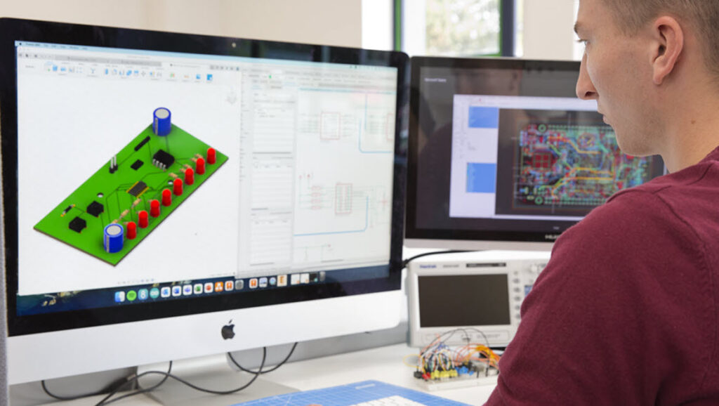
Fusion helps teams visualize PCB layouts within a 3D mechanical context, allowing fit, clearance, and integration requirements to be evaluated throughout development rather than only during final validation.
PCB manufacturing is not just about electrical correctness. A board needs to physically fit its enclosure, meet structural and thermal requirements, comply with manufacturing design rules, and be producible at the intended volume and cost.
Without ECAD-MCAD integration, teams typically encounter:
- Board outline mismatches: The PCB layout and mechanical enclosure evolve independently, and the mismatch is discovered late
- Component collision with mechanical features: A tall component placed correctly by electrical rules interferes with a boss, rib, or assembly feature
- Connector position conflicts: A port that shifted during routing no longer aligns with the panel cutout
- Thermal assumptions that fail in context: Heat dissipation modeled in isolation doesn’t account for airflow constraints inside the housing
- Manufacturing rework caused by late design data: The fabricator receives a design that hasn’t been validated against the mechanical build
With integration, teams validate fit and clearances as design progresses, not after it’s complete. Fusion maintains a live 3D board model that reflects the current layout, so mechanical designers always have accurate geometry to work against.
Layer stackup: the structural decision that affects everything
Layer stackup is one of the most consequential decisions in PCB design, and one of the earliest. The stackup determines impedance targets for controlled-impedance traces, dictates how power and ground planes are arranged, influences thermal performance, sets the board’s mechanical stiffness, and constrains the fabrication process.
A typical 4-layer stackup for a mixed-signal board:
| Layer | Function |
|---|---|
| Top copper | Signal routing, fine-pitch component placement |
| Inner layer 1 | Ground plane (reference for top layer signals) |
| Inner layer 2 | Power plane (VCC distribution) |
| Bottom copper | Signal routing, larger components |
For high-density or high-speed boards, 6- or 8-layer stackups are common, with additional dedicated signal layers and tighter dielectric control.
Key stackup decisions and their downstream effects:
Dielectric material and thickness: Determines the impedance of controlled-impedance traces. FR4 is standard for most applications; high-speed designs often require low-loss dielectrics such as Rogers 4350 or Megtron 6 to reduce signal attenuation at GHz frequencies.
Plane placement: Ground planes adjacent to signal layers provide the return path that keeps impedance consistent. Splitting a ground plane, or placing signal layers without a nearby reference plane, increases EMI and signal integrity risk.
Copper weight: Heavier copper (2oz or more) handles higher current on power layers but increases cost and can complicate fine-pitch routing on signal layers.
Symmetric construction: Asymmetric stackups cause bow and twist during reflow because the board expands unevenly. IPC-2221 recommends symmetric stackup construction for assemblies that go through reflow.
In Fusion, designers can define layer stackups, dielectric properties, copper weights, and board thickness early in the design process. These settings help establish the physical foundation for routing decisions and controlled-impedance design requirements before critical signals are placed.
Component placement: mechanical context from the start
Placement is where electrical and mechanical design intersect most visibly. The electrical goal is to minimize trace length, especially for high-speed nets. The mechanical goal is to fit the board into its enclosure, respect connector positions, and avoid component collision with housing features.
These goals often conflict. Resolving the conflict late, after routing is complete is expensive. Resolving it during placement is fast.
In Fusion, the PCB layout and the 3D mechanical model are live-linked. When you’re placing components in the electronics workspace, you can view the board inside its enclosure at the same time. Keepout zones derived from mechanical features appear directly in the layout view as constraints you can route and place against.
Placement priorities for manufacturability:
- Orientation consistency: Polarized components (electrolytic capacitors, diodes) oriented consistently reduce assembly errors and allow automated optical inspection to run with fewer exceptions
- Test point access: Place test points on a regular grid accessible to bed-of-nails fixtures or flying probe testers; tuck them under other components and they become inaccessible after assembly
- Thermal separation: High-dissipation components (voltage regulators, power FETs, motor drivers) placed near each other concentrate heat; distribute them or provide thermal relief
- Connector clearance: Connectors need clearance for mating cycles and, where applicable, for the cable bend radius behind the connector
The 3D board view in Fusion updates in real time as components are placed, so interference with enclosure features is visible before routing starts.
High-speed routing
High-speed design starts failing when routing is treated as a wiring exercise. At clock frequencies above 100MHz, and increasingly at lower frequencies as edge rates get faster, the physical properties of the trace matter as much as its connectivity.
Controlled impedance
Most high-speed buses (DDR, USB, PCIe, LVDS, Ethernet) specify target impedance values, typically 50Ω single-ended or 100Ω differential. Meeting those targets requires coordinating trace width, dielectric thickness, and dielectric constant, all of which come from the layer stackup.
Fusion applies impedance rules as routing constraints. Set the target impedance for a net class and the router flags traces that deviate from the calculated width for the selected layer.
Differential pair routing
Differential signals (USB, Ethernet, HDMI, PCIe) must be routed as matched pairs with consistent spacing and length matching. Skew between the positive and negative traces degrades the common-mode rejection that makes differential signaling immune to noise.
In Fusion, differential pairs are defined at the schematic level and routed as a unit. The router maintains pair spacing, and length tuning tools let you add serpentine sections to match lengths across a bus.
Return path management
Every signal has a return current. At high frequencies, that return current travels on the nearest reference plane, directly beneath the signal trace. Anything that interrupts the reference plane — a via antipad, a plane split, a cutout — forces the return current to detour, which increases EMI and crosstalk.
Practical rule: don’t route high-speed signals across plane splits. When you must cross a gap, place a stitching capacitor adjacent to the crossing point to provide a return path.
Via design for high-speed signals
Through-hole vias have stub inductance — the unused portion of the barrel below the last connected layer — that creates a resonance which can cause signal reflections at GHz frequencies. Back-drilling (removing the stub) or using blind/buried vias eliminates the problem.
Fusion supports the definition of various via structures used in modern multilayer PCB designs. Designers working on high-speed applications can evaluate the potential impact of via transitions, impedance discontinuities, and routing decisions as part of their signal integrity workflow.
Simulation: validating decisions before fabrication
Simulation is how you confirm that layout decisions that look correct actually perform correctly. Running it late, or skipping it, is where thermal problems first appear in physical hardware.
Thermal simulation
Thermal analysis helps engineers understand how heat moves through a PCB and the surrounding product.
Thermal performance depends on several factors including component power dissipation, copper distribution, board construction, airflow, enclosure geometry, and ambient operating conditions.
Within Fusion, PCB geometry can be evaluated alongside broader product design and simulation workflows, helping teams identify hot spots, assess thermal management strategies, and make informed design decisions before physical prototypes are built.
Design for manufacturability: catching problems before the fabricator does
DFM is the practice of designing a board that your fabricator and assembler can actually build reliably and at cost. Errors caught in DFM cost nothing. The same errors caught in fabrication or assembly can cost a full respin.
What makes a PCB design ready for manufacturing?
A design is ready for manufacturing when it satisfies three categories of requirements:
1. Fabrication rules
- Minimum trace width and spacing for the chosen fabrication class (IPC Class 2 or Class 3)
- Minimum drill size and annular ring for through-hole vias
- Copper-to-edge clearance to avoid trace exposure after board routing
- Solder mask expansion and slivers (narrow solder mask bridges between pads that can crack during assembly)
- Silk screen clearance from pads (silk screen printed on pads interferes with soldering)
2. Assembly rules
- Minimum component-to-component spacing for pick-and-place access and solder reflow
- Pad geometry appropriate for the soldering process (wave, reflow, selective)
- Fiducial markers for vision system alignment
- Panelization requirements if the board is designed for panel assembly
3. Test requirements
- Test points accessible to the in-circuit test fixture
- Bed-of-nails grid alignment if the test fixture uses a fixed probe layout
- Boundary scan or JTAG access for programmable devices
Fusion runs DFM checks as part of the design rule check workflow. Rules are configurable per fabrication class and can be matched to the specific capabilities of your contract manufacturer. The DRC output flags each violation by type and location, so issues are addressed systematically before Gerber generation.
How design errors typically show up in manufactured boards
The most common DFM failures in production:
- Solder bridges: Pads too close together, insufficient mask dam, or incorrect aperture in the paste stencil
- Open circuits: Thin traces damaged during etching, vias with insufficient annular ring that crack under thermal cycling
- Tombstoning: Small two-terminal components (0402, 0201 resistors and capacitors) that stand on one pad during reflow because the two pads heat unevenly
- Component misalignment: Footprint that doesn’t match the physical component, or placement offset that puts a fine-pitch device outside solder paste coverage
- Warpage: Asymmetric stackup or uneven copper distribution that causes the board to bow during reflow, leading to assembly failures
Many of these failures are detectable in the design file before a single board is fabricated. DRC and 3D visualization in Fusion surface them at the point where they cost nothing to fix.
How to avoid PCB design mistakes systematically
- Run DRC continuously during layout, not only at tape-out
- Use the 3D board view to check component clearances before routing locks placement in
- Generate and review a DFM report against your fabricator’s capability spec before releasing
- Get a fabricator DFM review on any new board design or new stackup
- Build AOI and X-ray inspection requirements into placement decisions early — designs that aren’t inspectable create field quality risk
PCB-enclosure integration: how the board and housing work together
A board that passes all electrical and DFM checks can still fail at the system level if it doesn’t fit its enclosure correctly.
The key integration points:
- Board outline and keepouts: The enclosure defines available board area; keepouts protect mounting bosses, vent locations, and cable routing channels
- Connector positions: Every external connector must align with a panel cutout; position errors require new tooling or manual rework
- Mounting hole locations: Holes must align with enclosure standoffs; misalignment puts mechanical stress on the board during assembly and use
- Component height clearances: Tall components (connectors, transformers, electrolytic capacitors) must clear the lid and any internal structure
In Fusion, PCB layouts and mechanical assemblies can be evaluated together within a connected design environment. Board outlines, mounting features, connector locations, and component clearances can be reviewed within the context of the complete product rather than in isolation.
When electrical or mechanical changes occur, teams can review their impact using shared 3D design data, helping reduce the version-control and communication challenges that often arise when ECAD and MCAD systems operate independently.
This approach helps teams spend less time reconciling exported geometry and more time validating product performance.
Manufacturing outputs: what a complete fabrication package contains
When the design is complete, manufacturing output generation produces the documentation the fabricator and assembler need to build the board.
Fabrication outputs:
- Gerber files (RS-274X): One file per copper layer, plus solder mask and silk screen
- Excellon drill files: Through-hole and, where applicable, blind/buried via drill data
- Board outline (DXF or Gerber): The edge cut defining the board perimeter
- Fabrication drawing: Layer stackup, material spec, surface finish, impedance requirements, IPC class
Assembly outputs:
- Bill of materials: Every component with reference designator, manufacturer part number, quantity, and placement side
- Pick-and-place file: Component centroids, rotation, and side for programming the placement machine
- Assembly drawing: Top and bottom views with reference designators, polarized component orientation marks, and critical assembly notes
Test documentation:
- Test point list: Net name, reference designator, X/Y coordinate, and accessible side for each test point
- Functional test procedure: Test sequence, stimulus and measurement for each verified parameter
Fusion generates all standard fabrication and assembly outputs from the PCB design file. BOM data is linked to the component library, so it reflects the current design without manual re-entry.
How electronics in Fusion connects the full workflow
Although PCB development is often described as a sequence of stages, real-world product development is iterative. Stackup decisions influence routing. Routing impacts thermal performance. Mechanical changes affect placement constraints. Manufacturing feedback can require multiple rounds of refinement.
The challenge isn’t completing individual tasks. It’s managing the dependencies between them.
Then keep the bullet list, but revise slightly:
- Schematic and PCB layout work from a connected design database
- PCB designs can be reviewed within a 3D mechanical context
- Mechanical requirements can inform board outlines and placement constraints
- Design rule checks and manufacturability validation help identify issues before release
- Manufacturing deliverables are generated directly from design data
For teams that currently rely on disconnected ECAD and MCAD workflows, the biggest benefit is often faster iteration. Electrical and mechanical decisions can be evaluated within the same product context, helping teams identify integration issues earlier and reduce the risk of costly late-stage changes.
Ready to get started with Fusion? Download a free 30-day trial today.
Frequently asked questions
A design is manufacturing-ready when it satisfies fabrication rules (trace widths, via annular rings, copper-to-edge clearances), assembly rules (component spacing, pad geometry, fiducials), and test requirements (accessible test points, inspection coverage). In Autodesk Fusion, DRC runs against configurable fabrication rules and flags each category of violation before Gerbers are generated.
Simulation helps engineers evaluate performance characteristics that are difficult or impossible to verify through visual inspection alone. Depending on the workflow, analysis may be used to investigate signal behavior, impedance consistency, coupling effects, thermal performance, and other factors that influence product reliability. Autodesk Fusion provides simulation capabilities that help teams identify potential issues earlier in the development process.
The enclosure defines the physical constraints the board must satisfy: available area, connector positions, mounting hole locations, component height limits, and thermal environment. Designing without accurate mechanical context produces boards that fit electrically but fail at the system level. Fusion electronics keeps the PCB layout and mechanical assembly synchronized, so enclosure constraints are visible during layout rather than discovered during integration.
Reliability is determined by decisions made throughout the design process. Layer stackup affects thermal management and mechanical robustness. Pad geometry and component orientation affect solder joint integrity through thermal cycling. Via design affects resistance to mechanical stress. Trace width and copper weight affect current-carrying capacity and resistance to electromigration. Fusion electronics DRC and 3D analysis surface the decisions that create reliability risk before the board is built.
Why is DFM important for PCB board design?
DFM errors caught before fabrication cost nothing to fix. The same errors caught in fabrication or assembly can force a respin. DFM covers three categories: fabrication rules (what your fab can build), assembly rules (what your assembler can populate and solder), and test requirements (what your test setup can reach). In Autodesk Fusion, DFM checks run against configurable rules matched to your fabricator’s specific capabilities.
The most common failures are solder bridges (pads or mask apertures too close), open circuits (thin traces or undersized via annular rings), tombstoning on small passives, component misalignment from footprint errors, and board warpage from asymmetric stackup construction. Most of these are detectable in the design file. DRC and 3D visualization in Autodesk Fusion identify them at the point where the fix is a rule change or geometry adjustment, not a fabrication respin.
Run DRC continuously during layout rather than only at tape-out. Use the 3D board view to validate component clearances before routing locks placement in. Generate a DFM report against your fabricator’s capability spec before releasing. Have your fabricator review any new stackup or new design before committing to a build. Design test access into the board from the start, not as an afterthought.
Effective collaboration means both teams work against shared, current geometry, not exchanged files. In Autodesk Fusion, the PCB layout and the mechanical assembly share a live-linked 3D model. Mechanical changes update keepout constraints in the layout automatically. Board changes are immediately visible in the enclosure assembly. Teams review the same 3D model rather than reconciling independently exported files.
Integration enables electrical and mechanical teams to work from connected design data rather than relying entirely on file exchanges at predefined milestones. This matters because many product development issues originate at the boundary between electrical and mechanical design, including connector alignment problems, enclosure clearance conflicts, mounting issues, and thermal constraints. Autodesk Fusion helps reduce this friction by bringing PCB and product design workflows together within a connected platform.
Stackup determines controlled-impedance trace widths, power and ground plane arrangement, thermal conductivity through the board, mechanical stiffness, and fabrication cost. It is one of the first decisions in the design process and one of the hardest to change late. Autodesk Fusion includes a stackup editor with impedance calculation, so targets can be confirmed before routing begins.
PCB design has a direct impact on thermal performance because the board itself acts as a heat-transfer system. Component placement, copper distribution, trace widths, board thickness, layer stack-up, and airflow paths all influence how effectively heat moves away from temperature-sensitive components. Poor thermal design can create hot spots that reduce performance, shorten component lifespan, cause signal integrity issues, or lead to premature product failure. Proper thermal management helps maintain reliability, improve efficiency, and reduce the risk of costly redesigns.
With Autodesk Fusion, thermal considerations can be evaluated earlier in the design process by combining PCB design, mechanical design, and simulation within a connected ECAD-MCAD workflow. Teams can assess how the PCB interacts with enclosures, cooling features, and surrounding components before manufacturing begins.
Several PCB design practices can help minimize heat buildup and improve thermal performance:
–Optimize component placement by separating high-power components and distributing heat sources across the board.
–Use thermal vias to transfer heat from hot components to internal or opposite copper layers.
–Increase copper area and copper thickness to improve heat spreading.
–Add heat sinks or cooling hardware for components with significant power dissipation.
–Design for airflow by considering enclosure geometry and cooling paths.
–Use wider traces and polygons for high-current circuits to reduce resistive heating.
–Select materials with appropriate thermal properties to improve heat dissipation.
–Validate thermal performance through simulation before prototyping.
Autodesk Fusion also supports design strategies such as via stitching, which can improve both electrical and thermal performance while maintaining manufacturability rules.
Fusion supports thermal analysis through its electronics cooling simulation capabilities. The software can simulate temperatures on PCB components, analyze heat distribution within the board and enclosure, and evaluate air temperature and airflow around electronic assemblies. This helps engineers identify potential overheating issues before physical prototypes are built.
Key capabilities include:
-Simulating component temperatures and identifying components at risk of exceeding temperature limits.
-Visualizing air temperature and air velocity within an enclosure.
-Comparing different cooling strategies, including heat sinks, fans, and enclosure designs.
-Evaluating thermal performance alongside the mechanical design because the PCB and enclosure exist within the same product development environment.
-Running cloud-based simulation studies without consuming local workstation resources.
A major advantage of Fusion is that thermal analysis is connected to the broader product development workflow. Because PCB layouts, electronics, enclosure geometry, and mechanical assemblies remain synchronized, engineering teams can evaluate thermal performance in the context of the entire product rather than treating the PCB as an isolated design. This helps identify issues earlier, reduce prototype iterations, and improve overall product reliability.
The biggest risks in PCB design are not usually found in the schematic. They emerge when electrical, thermal, mechanical, and manufacturing requirements fail to work together. Common risks include overheating, signal integrity problems, electromagnetic interference (EMI), poor manufacturability, component placement conflicts, and costly board re-spins. These issues can increase development costs, delay product launches, and reduce product reliability.
For teams developing connected products, another significant risk is disconnecting PCB design from the mechanical design process. When electronics and enclosure development happen in separate tools, fit, clearance, and integration issues may not be discovered until prototyping. Fusion helps reduce this risk by connecting PCB design, mechanical design, simulation, and manufacturing workflows within a shared environment.
Many PCB failures can be traced back to a handful of common design mistakes:
–Ignoring thermal management and failing to account for heat dissipation early in the design process. This can create hot spots that affect performance and reliability.
–Poor component placement, which can complicate assembly, increase noise, and create unnecessary thermal challenges.
–Inadequate signal integrity planning, particularly in high-speed designs where trace coupling, crosstalk, and electromagnetic interference can affect performance.
–Designing without manufacturability in mind, resulting in fabrication challenges, assembly defects, or higher production costs. Design for Manufacturability (DFM) is critical for moving efficiently from design to production.
–Insufficient grounding and shielding, which can lead to EMI and signal quality issues.
–Failing to validate designs before prototyping, increasing the likelihood of expensive board re-spins and project delays. Simulation and analysis can help identify problems before manufacturing.
–Managing electronics and mechanical designs separately, creating version-control issues and integration problems when board layouts and enclosure geometry evolve independently.
Fusion helps address many of these challenges through its connected ECAD-MCAD workflow, signal integrity analysis capabilities, and electronics cooling simulation tools. Designers can evaluate electrical performance, thermal behavior, and mechanical fit earlier in the development process, helping reduce errors before a board reaches manufacturing.
A typical PCB design workflow begins with defining the circuit requirements and creating a schematic that captures the electrical connections between components. Engineers then select components, verify circuit functionality, and move into PCB layout, where the physical board is designed. After layout, designers validate the design for manufacturability, signal integrity, thermal performance, and mechanical fit before generating manufacturing outputs for fabrication and assembly.
In Fusion, this workflow can remain connected from schematic capture through PCB layout, 3D PCB design, thermal analysis, manufacturing outputs, and product assembly. Because electronics and mechanical design share the same environment, teams can evaluate the PCB within the context of the final product rather than treating it as a separate file.
Typical stages include:
-Schematic capture
-Component and library selection
-Simulation and validation
-PCB layout and routing
-3D PCB review and ECAD-MCAD collaboration
-Thermal analysis
-Design for manufacturability (DFM) review
-Manufacturing and assembly documentation generation
The transition from schematic to board layout begins once the electrical design has been defined and validated. The schematic provides the logical representation of how components connect electrically, while the PCB layout converts that information into a physical board that can be manufactured. Designers place components, route traces between them, define power and ground structures, and optimize the design for electrical, thermal, and manufacturing requirements.
In Fusion, the schematic and PCB layout are connected, allowing engineers to move from circuit design into board design without recreating data in another application. The platform also supports bidirectional synchronization between schematic and PCB views, helping ensure that design changes remain aligned as projects evolve.
Because Fusion integrates ECAD and MCAD workflows, designers can also evaluate board placement, enclosure constraints, and mechanical clearances while the layout is being developed, helping identify integration issues earlier in the design process.
Schematic capture and PCB layout serve different purposes within the PCB design process.
Schematic capture focuses on electrical intent. It defines the circuit, components, and logical connections needed for the product to function. Engineers use schematics to verify the design concept and communicate how the electronics should operate.
PCB layout focuses on physical implementation. It determines where components are placed on the board, how traces are routed, how power is distributed, and how the design will be manufactured. PCB layout directly affects signal integrity, thermal performance, reliability, manufacturability, and overall product size.
A simple way to think about it is:
Schematic capture = what the circuit does
PCB layout = how the circuit gets built
Fusion connects both stages within a unified workflow, allowing schematic, PCB layout, 3D board visualization, mechanical integration, and simulation to remain synchronized. This helps reduce errors, eliminate data translation issues, and streamline the path from concept to manufacturing.