 Melisa Kaner
Explore how to move a PCB design from prototype to production with an overview of validation and component placement and how Autodesk Fusion streamlines these workflows.

Elevate your design and manufacturing processes with Autodesk Fusion
Moving from a functional prototype to a scalable production unit requires a rigorous approach to design validation and physical optimization. For engineering teams, the process involves a deep understanding of manufacturing constraints, thermal management, and signal integrity. Without this understanding, a design that works on a lab bench may fail in a high-volume assembly line if the layout does not account for automated pick-and-place tolerances or thermal dissipation requirements.
Therefore, high-quality PCB manufacturing requires designers to embrace Design for Manufacturing (DFM) principles. Autodesk Fusion simplifies the DFM process by consolidating advanced simulation, real-time design rule checking, and mechanical synchronization in a cloud-based workspace.
What makes a layout production-ready?
Successful PCB production requires engineers to design their layouts with manufacturing capabilities in mind. For example, designers need to validate copper trace widths, clearances, and annular rings against the specific tolerances of their selected fabrication house. Should these considerations be left unchecked, the final design may experience short circuits or compromised structural integrity during plating.
Performance is also impacted by DFM. In the case of high-speed signals, controlled impedance must be maintained by the fabrication house, and that directly ties to trace geometry. For that reason, engineering teams will routinely use simulation tools to analyze electromagnetic interference and signal coupling before committing to a physical build.
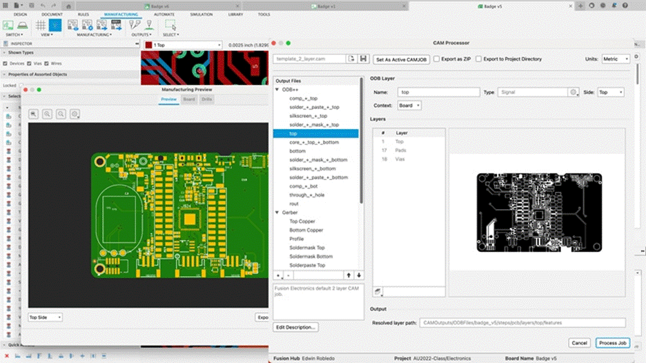
With respect to component placement, designers are expected to group components based on signal flow to minimize trace lengths and reduce parasitic inductance. For example, it is good practice to place high-power components away from sensitive analog circuits to prevent thermal interference and noise. Similarly, designers should orient components to facilitate automated soldering processes, such as reflow or wave soldering, and to provide adequate clearance for test points and mounting hardware.
The final output for a PCB designer is the Gerber files and the Bill of Materials (BOM). This contains information about every PCB layer, from solder masks to drill locations, in a format that fabrication machinery can interpret unambiguously. A design is truly production-ready only when teams have confirmed every physical and electrical constraint through a thorough design rules check.
PCB lifecycle with Autodesk Fusion
Autodesk Fusion provides a cloud-based environment where designers can manage the entire PCB lifecycle from a single platform.
With Fusion, the first benefit of an integrated workflow is that designers can move from schematic capture to PCB layout without the data loss that is typically associated with manual file conversions. The software maintains a live link between the electronic schematic and the physical board, meaning that all connections are synchronized throughout the iteration process. Such a high level of connectivity helps teams identify discrepancies early and reduce the risk of costly respins during the production phase.
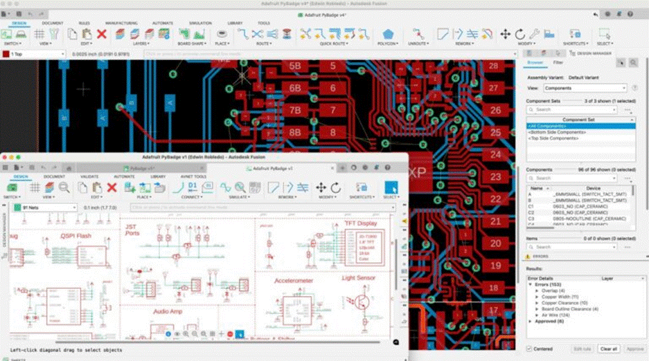
Using Fusion, engineering teams can also perform advanced SPICE simulations to verify circuit behavior in various conditions. With these tools, designers can virtually test signal integrity and thermal performance to ensure their design meets performance targets before reaching the factory floor. Meanwhile, the integrated Design Rule Check (DRC) mechanism helps teams input custom manufacturing constraints directly into the workspace. With DRC, Fusion automatically verifies that every trace meets the specific requirements of the chosen fabrication partner and indicates potential errors in real time.
Product teams can further optimize designs with Fusion’s native ECAD-MCAD integration, which lets designers visualize the PCB inside its mechanical enclosure in a 3D environment. Teams can check for mechanical interferences, verify connector alignment, and ensure that thermal management components, such as heat sinks, fit perfectly. By unifying the electronic and mechanical workflows, Fusion helps designers produce high-quality products faster and with greater confidence in their manufacturability.
The path to manufacturing excellence
Going into production is a complex process that requires collaboration and attention to detail. By focusing on DFM and strategic component placement, designers can guarantee that boards are reliable and cost-effective to produce. Fortunately, Autodesk Fusion provides engineering teams with the tools they need to validate designs, simulate performance, and unify workflows.
PCB manufacturing frequently asked questions (FAQs)
What makes a PCB design ready for manufacturing?
Why can a PCB prototype fail in production?
What is design for manufacturing (DFM) in PCB design?
How does component placement affect PCB manufacturability?
Why is validation critical before sending a PCB to production?
What files are required for PCB manufacturing handoff?
How do simulations help move a PCB from prototype to production?
How does Autodesk Fusion support PCB design validation?
Why is ECAD-MCAD integration important for PCB manufacturing?
How does an integrated PCB workflow reduce production risk?
What factors to consider when choosing PCB design software?
Autodesk Fusion is a strong choice because it combines schematic capture, PCB layout, 3D visualization, simulation, design rule checking, cloud collaboration, and mechanical design in a single platform. This allows electronics and mechanical teams to work from the same source of truth, reducing costly handoff errors.
Why can a PCB prototype fail in production?
Production failures can also occur when the PCB design is developed independently from the product enclosure. A board that works electrically may not fit correctly inside the final assembly, leading to mechanical interference, connector alignment problems, or cooling issues. Using simulation, design rule checking, and 3D validation early in the design process helps identify these issues before manufacturing begins.
Autodesk Fusion helps reduce these risks through integrated DRC, 3D visualization, thermal and signal analysis capabilities, and synchronization between electronic and mechanical design environments.
Is Autodesk Fusion good PCB design software?
One of Fusion’s biggest advantages is its ECAD-MCAD integration. Electronics and mechanical teams can work together in the same environment, allowing PCB layouts, enclosures, mounting points, and connectors to remain synchronized throughout development. This helps teams move from concept to manufacturing with fewer iterations and fewer design errors.
Why aren’t schematics enough to manufacture a PCB?
In other words, the schematic answers“what should connect?” while the PCB layout answers“how will it be physically manufactured?” A design cannot move into production without translating the schematic into a manufacturable board layout and validating it against manufacturing rules.
What does a PCB design include?
-Electronic schematics
-Component libraries and footprints
-Board outline and mechanical constraints
-Component placement
-Copper trace routing
-Vias and layer stack definitions
-Power and ground planes
-Design rule validation
-Manufacturing outputs such as Gerber files
-3D models for fit and clearance verification
Modern PCB development also includes simulation, version control, collaboration workflows, and integration with the mechanical product design process.
With Autodesk Fusion, designers can move from schematic capture to PCB layout, visualize the board in 3D, validate fit within the product assembly, and prepare manufacturing deliverables within a single connected workflow
How do PCB design and board layout stay synchonized?
Autodesk Fusion extends this synchronization beyond the PCB itself by connecting electronic and mechanical design data. Changes to the enclosure, board outline, mounting features, or component placement can be reflected across both ECAD and MCAD environments, helping teams avoid costly redesigns and maintain a single, accurate product definition.
Ultimately, this connected approach reduces design iterations, improves collaboration, and helps teams bring products to market faster.
How do mechanical and electrical teams collaborate effectively?
How do physical constraints affect PCB board design?
Common physical constraints include:
-Available space within the product enclosure
-Component height restrictions
-Connector and cable locations
-Mounting holes and fastening requirements
-Thermal management and airflow considerations
-Manufacturing and assembly requirements
Accessibility for testing, maintenance, or servicing
These constraints often create tradeoffs. A smaller enclosure may require a higher-density layout, while thermal requirements may demand additional spacing, copper pours, thermal vias, heat sinks, or airflow paths. As products become smaller and more complex, balancing electrical performance with physical limitations becomes increasingly important.
Autodesk Fusion helps engineers manage these constraints by allowing PCBs to be designed and reviewed within a 3D product context. PCB geometry can be derived from enclosure geometry, and changes made by mechanical or electrical teams can remain synchronized throughout development. This helps teams identify clearance, fit, and thermal issues earlier and reduce the risk of costly design iteration