Achieve reliable PCB layouts with optimal trace spacing—learn expert strategies and use Autodesk Fusion for error-free, manufacturable designs.
Elevate your design and manufacturing processes with Autodesk Fusion
Printed circuit boards (PCBs) are the foundation of electronics, powering everything from smartphones to industrial machinery. Yet, one of the most critical, and often overlooked factors in PCB design is trace spacing: the minimum distance between conductive copper traces. Get it wrong, and you risk short circuits, electromagnetic interference, manufacturing headaches, and even catastrophic failures. Get it right, and you unlock reliable performance, lower costs, and faster time-to-market.
This guide dives deep into the principles, standards, and best practices for PCB trace spacing, and shows how Autodesk Fusion empowers designers to master this essential aspect of circuit design.
Table of Contents
- Why PCB trace spacing matters
- Fundamental trace spacing rules and standards
- Minimum trace spacing requirements by application
- High voltage and safety considerations
- Manufacturing impact on trace spacing
- Signal integrity and electrical performance
- Thermal management considerations
- Design tools and implementation: Why Fusion excels at space tracing
- Best practices for trace spacing implementation
- Common design mistakes and how Fusion helps avoid them
- Autodesk Fusion —Your best solution for PCB trace cpacing
Why PCB trace spacing matters
Trace spacing is a design decision that impacts every aspect of your product’s performance and manufacturability. Here’s why it’s so important:
- Electrical isolation: Proper spacing prevents unintended current paths, reducing the risk of short circuits and electrical breakdown.
- Signal integrity: Adequate spacing minimizes crosstalk and electromagnetic coupling, ensuring clean, reliable signals.
- Thermal management: Spacing affects heat dissipation, especially in power circuits, helping prevent overheating and component failure.
- Manufacturability: Manufacturing capabilities and tolerances dictate the minimum achievable spacing. Designs that push these limits can drive up costs and reduce yield.
- Safety and compliance: High-voltage circuits require specific spacing to meet regulatory standards and prevent dangerous arcing.
Fundamental trace spacing rules and standards
The 3W rule: One of the most widely used guidelines is the 3W rule – the center-to-center distance between adjacent traces should be at least three times the width of the trace. For example, a 5mil trace should have at least 15mil spacing to the next trace. This rule helps reduce crosstalk to acceptable levels in most digital applications.
IPC standards: The IPC-2221 standard is the industry authority for PCB design, specifying minimum clearance based on voltage levels. For circuits below 30V, the minimum spacing is 0.13mm (5.1mil). As voltage increases, so does the required spacing—typically by about 0.1mm for every 100V.
Environmental factors: Humidity, contamination, and surface finish can all influence spacing requirements. External layers exposed to harsh environments need larger spacing, while inner layers protected by the PCB stack-up can often use tighter spacing.
Minimum trace spacing requirements by application
PCB trace spacing isn’t one-size-fits-all. Here’s how requirements vary by application:
- Low-voltage digital circuits: Standard logic circuits (3.3V, 5V) can use 4–6mil spacing, balancing density and reliability.
- High-frequency analog circuits:Sensitive analog signals require 6–10mil spacing to minimize crosstalk and distortion.
- Power circuits: Traces carrying significant current need 8–15mil spacing for safety, heat dissipation, and isolation.
- High-density designs: Mobile devices and wearables may push spacing down to 3.5–4mil, but this demands advanced manufacturing and increases costs.
- High-voltage circuits: Safety standards mandate clearances starting at 1mm for circuits above 50V, with creepage distances calculated based on surface path and environmental conditions.
High voltage and safety considerations
High-voltage PCBs introduce unique challenges. Clearance (straight-line distance) and creepage (surface path) must be carefully calculated to prevent arcing and ensure safety. Standards like IEC 60664 and UL 840 provide detailed requirements based on voltage, pollution degree, and material properties.
- Clearance: Minimum air gap between conductors; starts at 1mm for >50V and increases with voltage.
- Creepage: Path along the PCB surface; affected by humidity, contamination, and board material.
- Reinforced insulation: Safety-critical applications (medical, automotive) require dual barriers and increased spacing.
Manufacturing impact on trace spacing
Manufacturing capabilities are a major constraint on trace spacing. Here’s what you need to know:
- Etch factor: Copper etching creates angled sidewalls, narrowing spacing as thickness increases.
- Tolerances: Standard PCB manufacturing allows ±10% variation in trace dimensions, affecting final spacing.
- Production costs: Spacing below 4mil requires specialized processes, driving up costs and reducing yield.
- Quality control: Automated inspection systems verify spacing compliance, adding time and cost.
Use the largest practical spacing for your application. Many successful designs use 6–8mil spacing for most traces, reserving tighter spacing for critical high-density areas.
Signal integrity and electrical performance
Trace spacing directly affects signal quality, especially in high-speed digital circuits:
- Crosstalk: Electromagnetic coupling between traces can cause noise, timing errors, and data corruption. Spacing reduces coupling strength exponentially.
- Parasitic capacitance: Closer traces increase capacitance, affecting timing and power consumption.
- Impedance Control:
Differential pairs and high-speed signals require precise spacing for impedance matching. - Transmission Lines:
Microstrip and stripline configurations respond differently to spacing changes, impacting signal reflections and emissions.
Thermal management considerations
Heat dissipation is another reason to pay attention to trace spacing:
- Current-carrying capacity: Thicker copper and wider spacing allow higher currents without overheating.
- Thermal coupling: Closely spaced traces can create thermal shadows, reducing cooling effectiveness.
- Material selection: High-power designs may require materials with enhanced thermal properties and larger spacing.
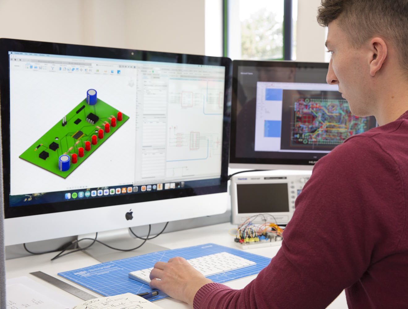
Design tools and implementation: Why Fusion excels at space tracing
Modern PCB design demands powerful tools to manage trace spacing rules, analyze performance, and ensure manufacturability. This is where Autodesk Fusion stands out:
Automated design rule checks
Fusion’s built-in rule checking system automatically verifies trace spacing throughout your design. Set up multiple net classes with different spacing requirements—digital, analog, power, high-voltage—and Fusion ensures compliance before you send your board to manufacturing.
Advanced simulation and analysis
Fusion integrates thermal simulation tools, allowing you to analyze the effects of trace spacing on crosstalk, impedance, and heat dissipation. Optimize your design for performance and reliability, not just manufacturability.
Collaboration and DFM integration
Fusion’s cloud-based platform makes it easy to collaborate with manufacturers and team members. Share designs, apply real-world constraints, and get feedback directly in your workspace. This tight integration helps you avoid costly redesigns and ensures your spacing choices are practical and cost-effective.
Flexible rule management
Set up custom spacing rules for different circuit sections, and let Fusion manage them automatically. Whether you’re routing high-speed signals, power nets, or analog traces, Fusion keeps your design organized and error-free.
Automatic and manual routing
Fusion’s routing tools apply spacing rules consistently, but also allow manual optimization for critical sections. Combine the speed of automatic routing with the precision of manual control for the best results.
Best practices for trace spacing implementation
- Collaborate early: Work with manufacturers to understand achievable spacing limits and associated costs.
- Progressive spacing strategy: Use larger spacing wherever possible; reserve tight spacing for space-constrained areas.
- Document critical Areas:
Highlight special spacing requirements on fabrication drawings. - Test and Validate:
Use electrical testing and inspection to verify spacing performance in final products. - Consider Environmental Factors:
Adjust spacing for humidity, contamination, and conformal coating processes.
Common design mistakes and how Fusion helps avoid them
- Insufficient spacing: Causes manufacturing yield issues and safety hazards. Fusion’s rule checks catch these errors early.
- Overly conservative spacing: Wastes board space and increases costs. Fusion’s simulation tools help you find the optimal balance.
- Inconsistent rules: Leads to manufacturing confusion. Fusion’s rule management ensures consistency across your design.
- Ignoring environmental factors: Can cause field failures. Fusion’s integrated analysis tools help you account for real-world conditions.
Autodesk Fusion —Your best solution for PCB trace cpacing
PCB trace spacing is a critical factor in circuit reliability, performance, and manufacturability. With shrinking form factors and increasing complexity, designers face tough trade-offs. Fusion provides the tools, automation, and collaboration features you need to ensure your designs are robust, cost-effective, and ready for production.
Ready to design with confidence? Choose Fusion for smarter, safer, and more efficient PCB layouts.