This post is also available in:
If you have even a little bit of interest in learning about electronics, then you absolutely need to know about the printed circuit board or the PCB. Why? These boards are in every piece of electronics known to man, no exceptions! Open your computer, smartphone, or even a fork, and you’ll find a PCB.
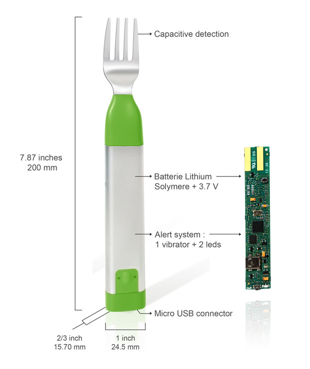
To the electronics beginner, these green shapes can seem a bit mysterious at first. There’s a ton of different looking components, and so much to learn to know how it all works together. But with a high-altitude perspective, understanding what a PCB is and how it works can be easy. Look at a PCB from 10,000 feet, and you’ll find that it looks just like a city!
Take the Window Seat
Although not lately, likely you’ve flown in an airplane at least once in your life. My favorite part of the journey is when the plane takes off from the runway. As you climb higher and higher, you get a new perspective on a city that you only see from the great heights. And the higher you go, the more you start to see just how your city is organized and meticulously planned. There are roads, buildings, cars, and people all connected in a complete system.
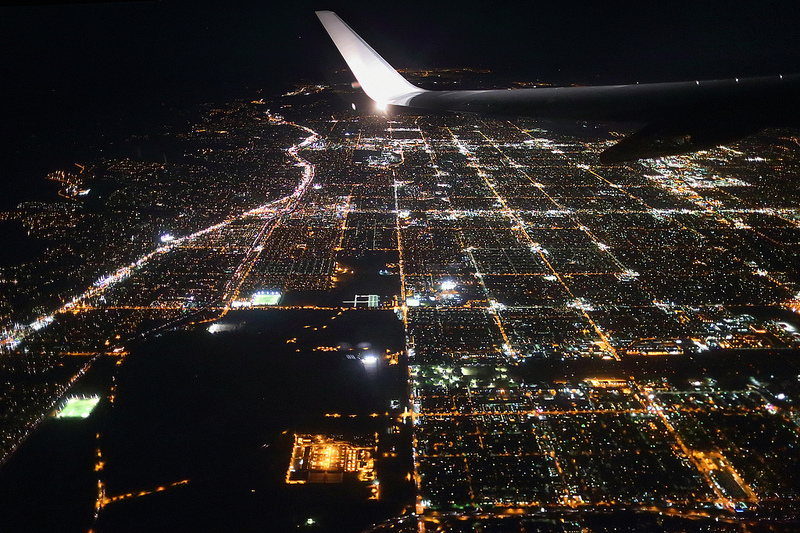
Just like our cities, circuit boards provide a complete system, a foundation, for all of the electronic components that make our everyday devices come to life. In fact, you can compare many aspects of a city to a PCB.
Traces = The Roads
On a PCB, you’ll notice a bunch of lines running all over the place, connecting to various components. These are just like the roads in our cities, except instead of cars zipping around, electrons are flying down streets made out of copper, hurrying off to power one component after another! These copper roads are called traces in our PCB city.
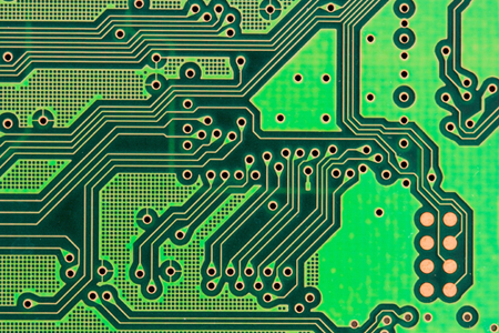
A PCB without any of its components, you can see the traces connecting everything.
Integrated Circuits = The Downtown
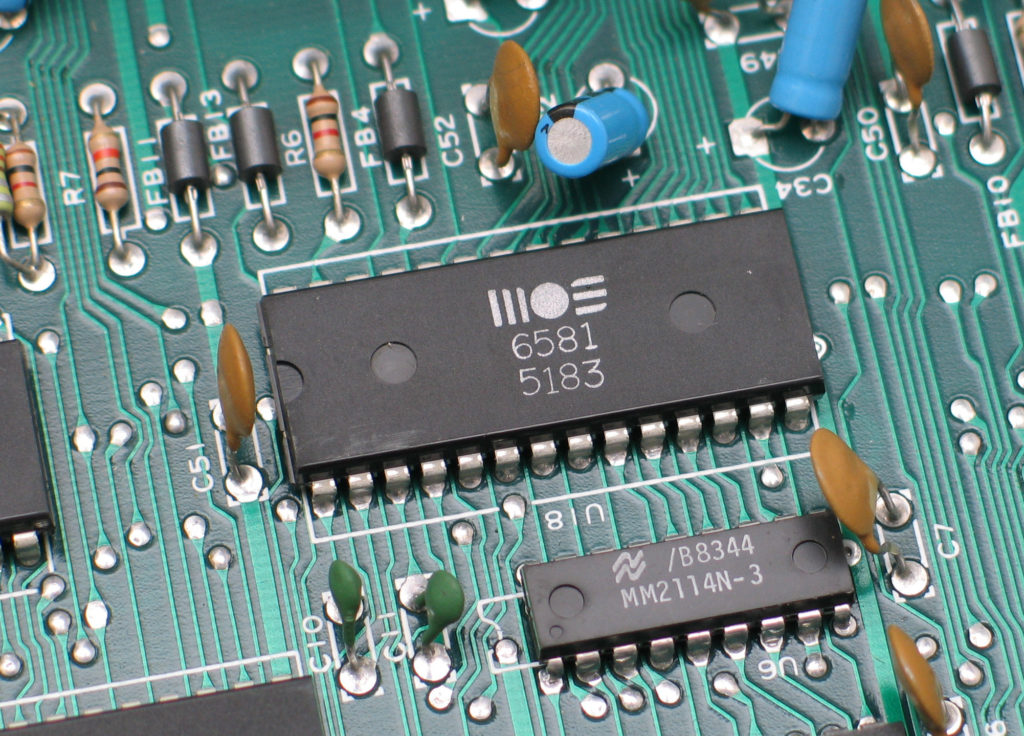
Downtown is where all of the work in a city happens. You’ve got your big corporate offices, local business on every corner, and maybe even some open markets. This central hub of human activity is just like those square black shapes that you’ll find on a PCB called Integrated Circuits (IC). These ICs are where all of the heavy processing happens in a PCB, doing rapid-fire calculations.
Passive Components = The Suburbs
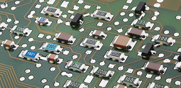
In the suburbs are where homes, parks, and schools are a common sight. From a plane, you’ll notice that the rows of houses in a suburb often look just like the small resistors or capacitors found all over a PCB. These resistors are out there, resisting the flow of current according to their value.
Pads = The Construction
No city is free from construction! Whether it’s building a new skyscraper or a new apartment complex, you’ll find new foundations being laid everywhere. These foundations are just like the empty pads that you’ll find on a PCB with no components on it. While they might be empty now, a component will soon be soldered to them.
Silkscreen = Addresses & Street Names
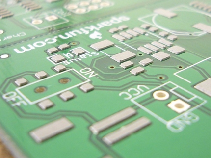
You won’t find your way around a city without some address or street name. And just like how these two help you to navigate mazes of streets, all of the white writing that you find on a PCB does just the same. This lettering, called silkscreen, helps people that are assembling or fixing PCBs to know exactly what a part is and its location.
Vias = The Sewer System
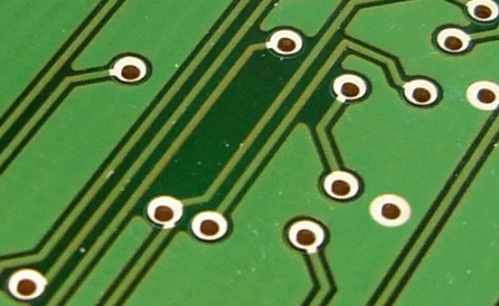
All of that water that we use when doing the dishes or washing our car has to go somewhere, and into the sewers, it finds itself traveling to new destinations. The sewer system is just like the holes you might find on a PCB called vias. These manhole-like shapes help to deliver electricity from one side of a PCB to another, just like how water travels from your sink to the local sewage plant, it’s an expressway!
Capacitors = The Power Plant
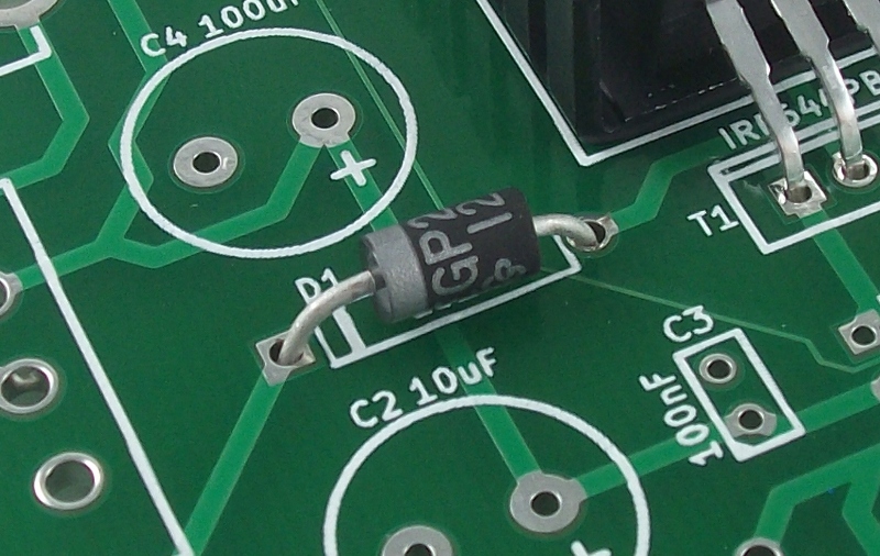
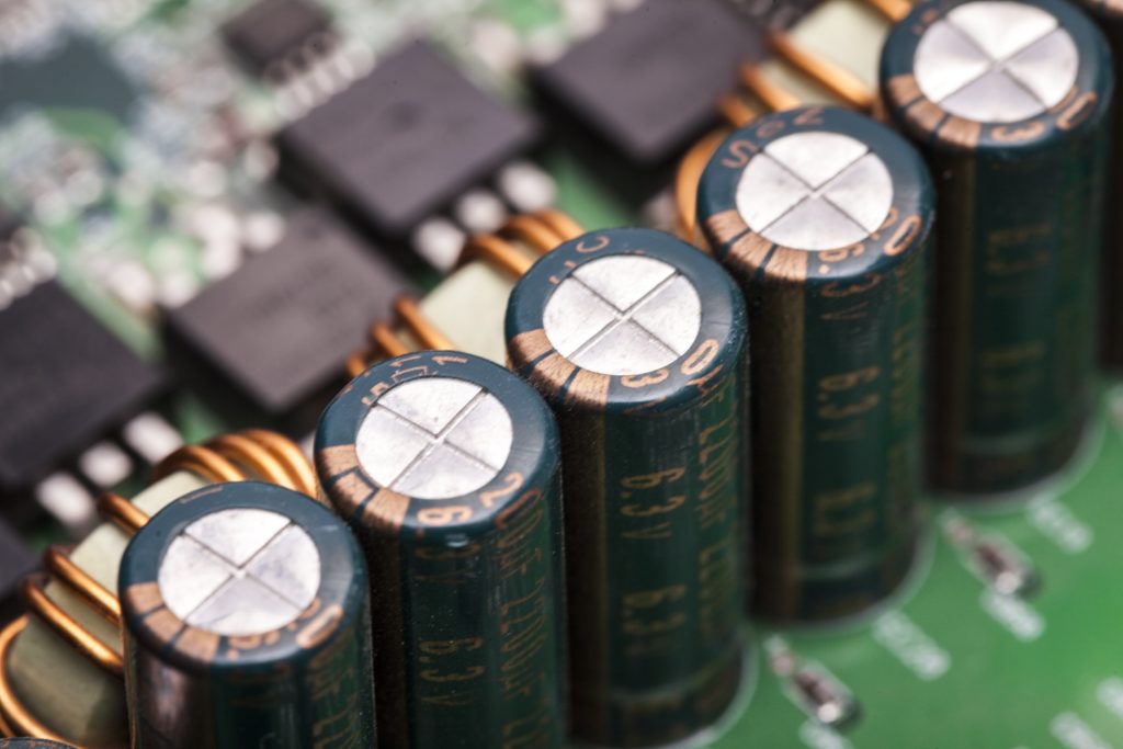
Power plants keep our lights running. Could you imagine what a city would be like without any? Hopefully, not zombie-infested! Just like power plants in a city, we have what are called capacitors on a PCB that store electricity. They can hold a charge, and release it when needed to send power where it needs to go.
LEDS = Street Lights & Signs
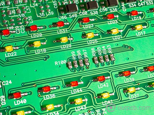
Street lights and signs help to keep order in a world full of crazy drivers, controlling the flow of traffic in our maze of streets and highways. On a PCB, streetlights and signs are just like diodes and their cousin the LED. The diode controls the flow of electricity on a PCB, allowing it to go only in one direction. And you’re bound to have seen a LED, it’s just like a diode, except that it lights up when current runs through it.
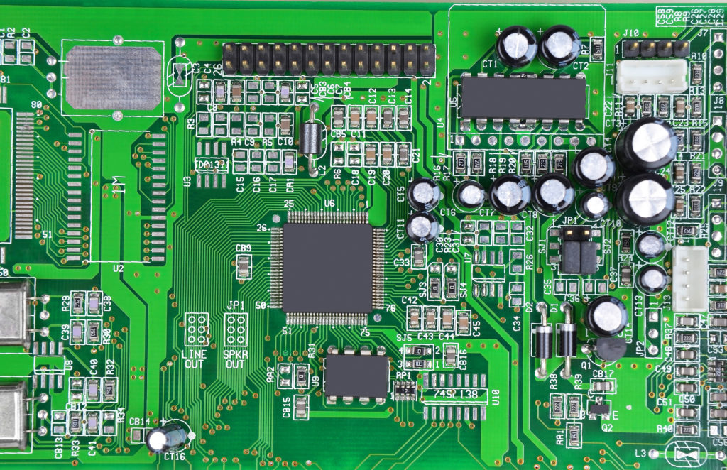
Now that you have all the individual parts put together in your mind, check out the picture below to see if you can point out some of the landmarks on this here PCB. Integrated circuits are the easiest to find; just look for the black boxes. But you might need to squint to see all of the tiny resistor suburbs grouped all over the place. Of course, the parts and pieces we listed above are only a fraction of the things you’ll find on a PCB, but you’ve got enough knowledge now to yank the PCB out of any piece of electronics and start naming things!
How would I make a PCB?
You can think of a PCB as a kind of delicious, multi-layered vanilla and strawberry cake when looked at from the side. It has several repeating layers of copper, solder mask, silkscreen, and fiberglass. Let’s start from the inside out to understand these layers.
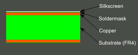
A cross-section of a double-sided PCB with silkscreen, solder mask, copper, and FR4.
Fiberglass. This material rests at the center of a PCB and is commonly referred to as a substrate, or FR4. The fiberglass is the strongest layer of them all and is responsible for giving a PCB it’s rigid and thick structure. When making a PCB, the entire process starts with the fiberglass, and all the other layers are added on top.
Copper. Without a layer of copper, a PCB would never be able to conduct electricity. You’ll usually find copper on both the top and bottom of a PCB, and it contains all of the traces that will connect your components.
Soldermask. This stuff is what gives a PCB its traditional green color and is applied over the copper layers. You might also find PCBs in red or blue; it’s the designer’s choice! Solder Mask holds an outstanding job of keeping all of the copper traces insulated from each other so no accidents can occur like short circuits.
Silkscreen. You’ll find this white text all over the place on a PCB, identifying the names of resistors, capacitors, LEDs, etc.… Silkscreen comes in handy when you’re making a PCB, as it can tell another human or computer where a particular part needs to go.
The actual process of how a PCB is made can be complicated, and involves the use of a manufacturer, also called a fab house by some. These fab houses will take all of the completed design files that an engineer hands off to create a PCB in its physical form. While the entire process is deserving of its own blog post, we’ll keep things simple with a brief outline of how a PCB comes to be:
- Step 1 – Creating a fiberglass foundation. A manufacturer will first make the inner fiberglass layer (core) that all of the other layers of copper, solder mask, etc.. will be applied to.
- Step 2 – Adding copper layers. With the fiberglass foundation in place, a manufacturer will then add copper foil on both sides of the fiberglass.
- Step 3 – Adding copper patterns. Next, a laminated sheet of the PCB design is laid on top of the copper, which shows where all of the copper traces need to be.
- Step 4 – Defining copper patterns. The laminated sheet and copper are then exposed under a UV lamp and covered with a photoresist film, which etches the traces into the copper foil.
- Step 5 – Bathing the board. Now that the copper traces are in place, a PCB will then be given a chemical bath that removes all of the unwanted copper, leaving only the copper traces that an engineer designed.
- Step 6 – Protecting with solder mask. A protective layer of solder mask is applied, giving a PCB its traditional green color while protecting it from short circuits.
- Step 7 – Adding silkscreen. To finish up, white silkscreen is added, which will help to know precisely where components need to go on a PCB. At this stage, the PCB is considered complete as a “bare board,” meaning it has no parts attached yet.
- Step 8 – Adding components. The bare board is then taken through an assembly process where various components like resistors, integrated circuits, capacitors, etc. are attached. Once complete, this is the PCB in its final form that you’ll see in all of your electronics at home.
The assembly process has quite a few details that we left out and is a world in itself. If you’re interested in learning more about the manufacturing process, be sure to check out the video below to see it in action at Eurocircuits!
Were PCBs Always This Complex?
The green PCBs that we have come to know in all of our electronics have not always been so. Why, just over 60 years ago, you were bound to see PCBs made from materials like masonite, cardboard, and even wooden planks. In these old-school PCBs, flat brass wires were bolted onto the board, and a collection of components were scattered all over the place. Here’s an old TV with one of the earliest PCBs inside, look at that mess!
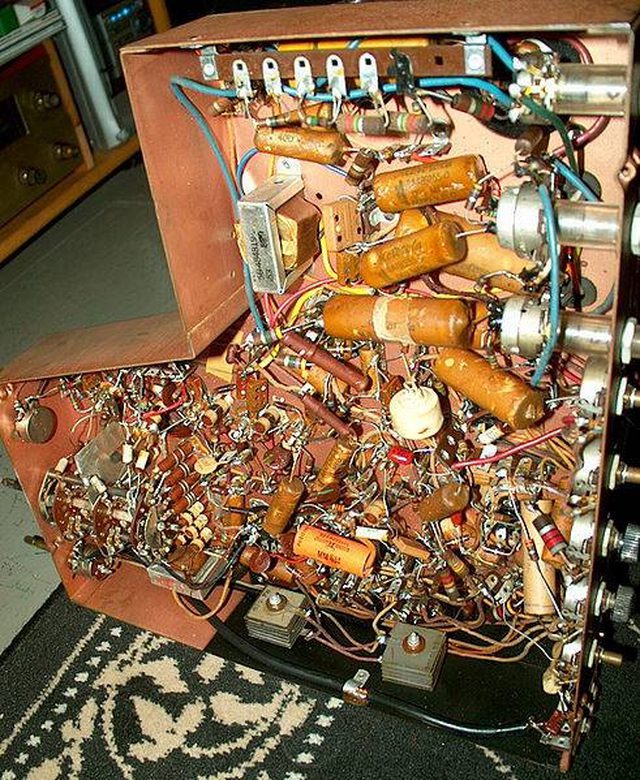
This monstrosity of a PCB soon changed, though, and in 1943 Austrian scientists Dr. Paul Eisler created the first modern PCB for a radio. Soon after, copper replaced brass the metal of choice for PCBs, as it allowed electricity to flow more efficiently, and it was also a lot cheaper to manufacture.
The PCB finally got its moment of fame in 1956, when the US Patent Office issued a patent for the “Processing of Assembling Electrical Circuits” to a group of scientists in the US Army. It’s the military that is to be thanked for many of the advancements we’ve seen in PCBs. Thanks to their need for new weapons and communications systems, we’ve taken the hulking mass of PCBs of yesterday and shrunken it down into something that can fit into our pockets!
Today’s Wild and Crazy Uses for PCBs
Today, PCBs are all over the place, powering some of the wild and crazy gadgets and services that we could have ever imagined existing. Have you heard of these?
Delivery Drones
Amazon unveiled its new delivery service in 2017, Prime Air, made possible by drones! We’re talking about being able to order something off Amazon and have it delivered to your home in mere minutes, not days, all thanks to the power of PCBs.
The PCBs in these drones deliver all of the complexity needed to get the job done, including GPS and Bluetooth that allow a package to be delivered with precision, and gyroscopes, and accelerometers that keep them flying straight. Check out the video below to see Amazon Prime Now in action.
Prosthetic Limbs
Gone are the days of plain mechanical limbs that didn’t provide any feedback. Today’s prosthetic limbs are packed with microprocessors that are adding a whole new level of a natural experience. In prosthetic legs, knee angle sensors can provide information to a microprocessor about pressure adjustments in the heel or front part of the foot. This all leads to a much more natural walking experience thanks to PCBs and their microprocessor counterparts.
Hearing Implants
Cochlear Implants allow the deaf or hearing impaired to hear again, all thanks to the power of PCBs and electronics. These implants are placed surgically under the skin and contain a ton of electronics, including:
- A microphone that picks up all the variety of sounds from an environment.
- A speech processor that can make sense of all the sounds collected by the microphone.
- A transmitter, receiver, and stimulator that receives signals from the speech processor and converts them into electrical impulses.
- An electrode array which collects all of the electrical impulses from the stimulator and sends them to regions of the auditory nerve to be heard!
These are just a few of the extraordinary uses that PCBs and electronics as a whole have made possible for the human race. There’s a ton more out there, like the computer or smartphone that you’re reading this blog post on. Without a PCB, you would never be here! Hats off to you again, PCB.
You are Free to Walk About Your PCB
The PCB is the foundation for our future, allowing us to create, discover, and improve the human experience in ways we might have never thought possible. But today, we’re just at the beginning of our journey with PCBs. In the future, we might find ourselves using biodegradable circuit boards to help eliminate electronic waste. Or perhaps you’ll be able to 3D print your own PCB from the comfort of your home!
There are so many uses to electronics and PCBs, and it all starts with you! Your bright engineering mind probably has some ideas up there; it needs to get out. Why not use a tool to bring those ideas to life that millions of other engineers trust every day? Try Autodesk Fusion 360 today!