Explore the technical distinctions between PCB design and PCB board design. It examines how integrated workflows and physical layout constraints shape the development of electronic products for engineering teams.
Elevate your design and manufacturing processes with Autodesk Fusion
Electronic product design requires a balance between developing circuits that are functional and ones that can be manufactured in reality. While teams frequently use the terms “PCB design” and “PCB board design” interchangeably, there is a distinction between the high-level engineering of a circuit and the specific layout of the physical hardware. Designers need to understand this difference to better manage the move from a conceptual schematic to a tangible, manufactured product.
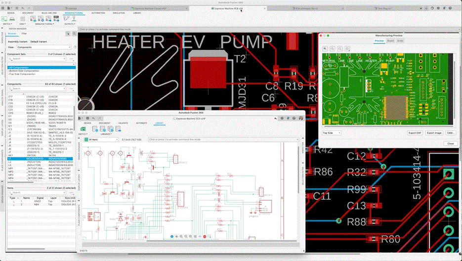
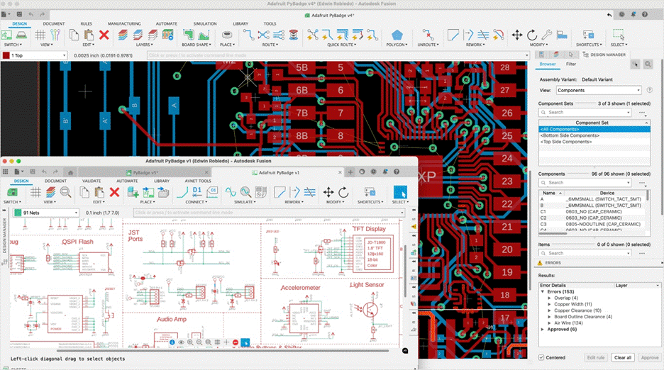
Autodesk Fusion enables designers to manage both sides of the problem within a single, connected platform.
PCB design versus PCB board design
PCB design is the end-to-end engineering process of creating electronic circuits. This workflow begins with schematic capture, where designers define the electrical connections and logical relationships between components. In this phase, teams focus on system intent, signal requirements, and component selection to ensure the circuit performs its intended function on the lowest level.
PCB board design, on the other hand, focuses on the physical implementation of the board itself. Here, the focus is more on manufacturing, as teams prioritize layout, component placement, and board shape. This process involves translating the logical connections from the schematic into a physical structure that adheres to mechanical limitations. Designers must account for the substrate’s physical dimensions and the specific layering of copper and insulation.
The physical design phase introduces constraints such as trace width, clearance, and thermal management that do not exist in a digital schematic. Here, engineers need to determine trace widths based on current-carrying requirements to prevent overheating or board failure. As a result, designers need to manually route traces to prevent short circuits and signal interference. This process requires complex spatial calculations, where every millimeter of copper affects the performance of neighboring signals.
These challenges are exacerbated in high-speed circuits. In a schematic, a connection is a simple line, but on a physical board, that line becomes a transmission line with resistance, capacitance, and inductance. Designers need to implement differential pairs and length-matching to ensure signals arrive at their destinations simultaneously and without distortion. These physical realities require a different set of technical skills than those used for schematic design.
Integrating workflows with Autodesk Fusion
With Autodesk Fusion, teams can unify schematic design and board layout within a single platform. Specifically, Fusion helps designers eliminate manual handoffs and data translation issues that introduce errors in the development cycle by automatically applying changes to the electrical schematic to the board’s layout, and vice versa. In that way, the end-to-end design workflow stays connected and cohesive.
For mechanical constraints, Fusion offers tools that help designers identify clearance issues and component interferences early in the design process. For example, product teams can use Fusion’s integrated 3D visualization capabilities to analyze how the PCB fits within a mechanical enclosure. Using these features, manufacturing teams can verify that the physical board design meets all mechanical requirements before sending files to production.
Designers can also use Fusion to perform detailed simulations that verify their design’s performance before manufacturing. For example, Fusion includes SPICE simulation that helps verify circuit behavior based on the schematic, while signal-integrity tools help designers analyze layouts and high-speed traces. Using these analysis features, designers can predict how the board will function under real-world conditions. This helps reduce the number of physical prototypes and board respins required to reach a final product.
The future of electronics design
Professional designers need to master both the logical intent and physical layout of electronics to build products that perform reliably. Autodesk Fusion enables teams to master both PCB design and PCB board design with a single cloud-connected workflow. By managing the entire development process in a single tool, designers can focus on creating high-performance electronics that define the next generation of technology.