 Edwin Robledo
This blog discusses the importance of circuit design in developing consumer electronics, detailing its challenges and impact on product functionality. It also highlights how Autodesk Fusion assists engineers by integrating mechanical and electrical design, optimizing workflows, and enhancing collaboration for more efficient product development.

Elevate your design and manufacturing processes with Autodesk Fusion
Circuit design is a fundamental process in modern product development, especially in the creation of consumer electronics. From smartphones to wearables, circuit design is at the heart of nearly every product we use today. As devices grow smaller, more powerful, and more interconnected, the need for efficient and precise circuit design has never been greater. This blog explores circuit design’s role in consumer product development and how Autodesk Fusion can streamline this critical process.
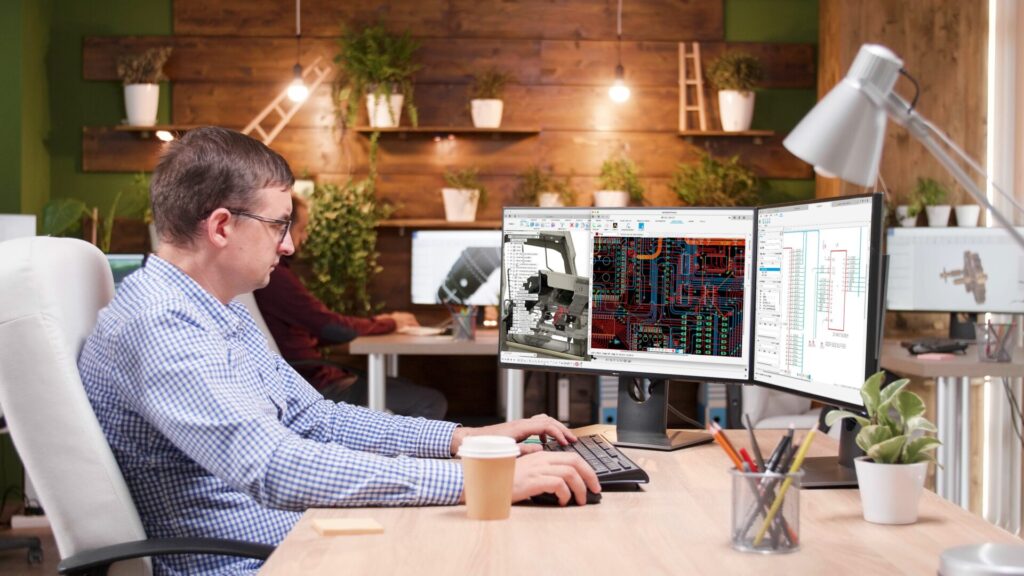
Circuit design in product development
Circuit design is the process of creating the electrical pathways that allow a device to perform its intended functions. Circuits enable the flow of electricity through a device, connecting components such as microprocessors, sensors, and power supplies. Without a well-designed circuit, even the most advanced components would be unable to work together effectively.
One central aspect of circuit design is the development of schematics and layout designs. The schematic represents a symbolic diagram of the circuit, showing how components are interconnected. Once the schematic is created, the layout process determines the physical arrangement of these components on a printed circuit board (PCB). This is a highly detailed process that involves considering factors such as trace routing, signal integrity, and thermal management.
Modern challenges
Often, consumer product development begins with conceptualizing a product’s core features, which drives the requirements for the circuitry. Whether the product is a fitness tracker or a smart thermostat, engineers must ensure that the circuit meets the necessary power, size, and performance specifications. The complexity of circuit designs has increased as products are increasingly expected to do more with less space and energy.
For example, miniaturization is a challenge. Designers must fit more powerful components into smaller devices while also ensuring that these components do not overheat or interfere with one another. Additionally, modern products often require wireless communication capabilities, which add layers of complexity to the circuit design process. Engineers must carefully balance these various requirements while optimizing for performance, reliability, and cost.
As devices become more complex, circuit designers must also consider regulatory standards, product safety, and reliability over the product lifecycle. From electromagnetic interference (EMI) mitigation to thermal management, a successful circuit design must address all aspects of performance in real-world conditions.
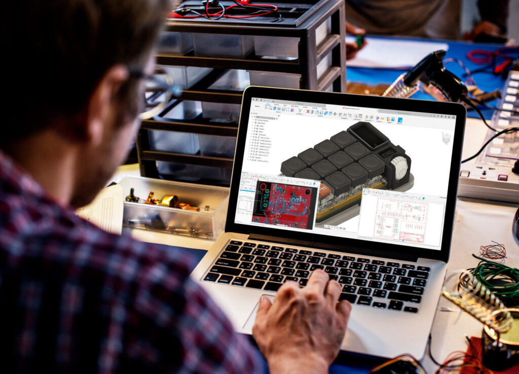
How Autodesk Fusion supports circuit design
When it comes to circuit design, Autodesk Fusion provides an integrated development environment that simplifies engineering and product design. Its ability to handle both mechanical and electrical designs within the same platform allows for smoother collaboration between teams. The tight integration between electronic and mechanical design is a powerful advantage. This is especially important where the fit and functionality of a circuit within a product’s enclosure are critical considerations.
Electronics workspace
One of the unique features in Fusion for circuit design is its electronics workspace, which includes schematic design, PCB layout, and component library management. Engineers can easily create and edit circuit schematics, selecting from a vast library of pre-designed components. This central tool helps speed up the design process while also guaranteeing accuracy and consistency in component selection. Meanwhile, the ability to directly import components into the design environment reduces manual errors and streamlines the workflow.
PCB tools
The PCB layout tools in Autodesk Fusion are particularly valuable when designing products with space constraints, such as wearable devices or smartphones. Designers can visualize the physical placement of components and make adjustments to optimize for size, thermal performance, and signal integrity.
Electronic simulation
Another important feature is the integration of simulation tools within Fusion. Simulation allows engineers to test their circuit designs under various conditions before moving into physical prototyping. By running simulations for thermal behavior, signal integrity, and electromagnetic interference, designers reduce the likelihood of errors and costly rework during later stages of development.
Collaboration
Furthermore, Fusion’s collaboration tools provide a centralized platform for managing design iterations and feedback from multiple stakeholders. Engineers can review circuit designs in the context of the overall product so that all design aspects—from mechanical enclosures to electrical connections—are aligned. Such a holistic approach reduces design conflicts and enhances overall product quality.
A future for circuits
As products become more complex and compact, the demands on circuit design continue to grow. Autodesk Fusion offers robust tools for streamlining the design process and allowing engineers to create efficient, reliable, and cost-effective circuits for the next generation of consumer products.
Frequently asked questions
The best circuit design tools help engineers move efficiently from concept to manufacturable hardware while reducing errors and rework. Key features include schematic capture, component libraries, simulation capabilities, PCB layout, collaboration tools, and integration with mechanical design workflows. These capabilities help teams validate designs earlier, improve reliability, and accelerate product development.
For modern electronics development, integration is increasingly important. Rather than treating electronics as a standalone activity, many teams need tools that connect circuit design with PCB layout, mechanical design, simulation, manufacturing, and data management. Autodesk Fusion combines these capabilities in a unified platform, allowing electronics and mechanical teams to work from a shared product definition.
Important capabilities to look for include:
-Schematic capture and circuit design
-Component and library management
-SPICE or circuit simulation
-PCB layout and routing
-Thermal analysis
-ECAD-MCAD collaboration
-Manufacturing output generation
-Version control and cloud collaboration
-Design for manufacturability (DFM) support
PCB design software should support the entire electronics development workflow, not just board layout. At a minimum, it should provide schematic capture, PCB layout tools, design rule checking, component management, and manufacturing outputs. For more complex products, simulation, signal integrity analysis, thermal analysis, and mechanical integration become increasingly important.
Modern PCB design software should include:
–Schematic capture to create and validate circuit designs.
–PCB layout and routing tools for designing board geometry and interconnections.
–3D PCB visualization to evaluate fit within the final product.
–Design rule checking (DRC) to identify manufacturability and reliability issues.
–Thermal analysis to identify overheating risks before prototyping.
ECAD-MCAD integration to keep electronics and mechanical designs synchronized.
–Manufacturing outputs such as Gerber files, assembly documentation, and BOMs.
–Cloud collaboration and data management to support distributed engineering teams.
Autodesk Fusion includes these capabilities within a connected design environment, enabling teams to move from schematic design through PCB layout, 3D visualization, simulation, manufacturing preparation, and product assembly without relying on disconnected tools.
Yes. Modern cloud-connected PCB design platforms can support complex multilayer PCB designs used in consumer electronics, industrial equipment, communications devices, and embedded systems. The ability to design multilayer boards depends on the capabilities of the PCB software rather than whether the platform is cloud-based.
Cloud-based tools offer additional advantages, including centralized data management, version control, collaboration, and access to the latest design information from anywhere. These capabilities can be particularly valuable for distributed teams developing complex products that require close coordination between electronics and mechanical engineering.
Autodesk Fusion supports professional PCB development workflows and connects PCB design with 3D mechanical design, simulation, manufacturing preparation, and product data management. This allows engineers to develop multilayer PCB designs while keeping electrical, mechanical, and manufacturing requirements aligned throughout the product development process
Yes. Autodesk Fusion is a professional and capable PCB and circuit design platform that combines schematic capture, PCB layout, ECAD-MCAD integration, thermal simulation, and manufacturing preparation in a single environment. It is particularly well suited for teams developing electronic products that require close coordination between electronics, mechanical design, and manufacturing.