Discover via stitching’s crucial role in PCB design, its types, implementation, and benefits in enhancing performance and managing heat.
Introduction to PCB design
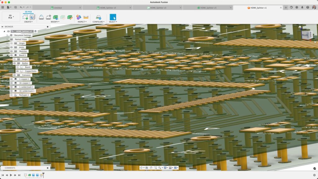
Printed Circuit Board (PCB) design is a complex process that serves as the foundation for modern electronics. At its core, PCB design involves crafting a detailed blueprint to ensure reliable electrical connections and optimal performance for all components. A crucial element of this process is the effective distribution of power and ground signals across the board. This is achieved by incorporating dedicated ground and power planes—large copper layers providing a low impedance path for electrical currents. These planes stabilize voltage levels, minimize noise, and enhance signal integrity throughout the board.
Elevate your design and manufacturing processes with Autodesk Fusion
Another significant challenge in PCB design is thermal management. Electronic components generate heat during operation, which, if not properly managed, can degrade performance or even damage sensitive parts. Techniques such as via stitching are vital in addressing this issue. By placing multiple vias in a grid pattern, designers create robust vertical connections between different layers. It ultimately allows for efficient heat dissipation. This method helps maintain minimal temperature rise and supports the overall goal of improved signal integrity, and long-term reliability of the PCB.
Why do we need via stitching?
Before we delve into the details of via stitching, let’s first understand what a via is. During the production stage of a PCB, a hole is drilled through its base material to create a via. This hole is then filled with copper on the inner layer, enabling it to transmit copper traces across multiple layers of the PCB.
However, via stitching uses multiple Vias to drill and connect copper areas on different layers of the PCB. Via stitching is often used to connect copper pours or copper pour regions to ground. This process improves grounding and thermal management. Typically, designers apply this technique to larger copper planes, such as ground filling planes, power planes, and copper pourts. This application enhances the ground return paths in the PCB from load devices to the power source.
Why is stitching that important?
The significance of via stitching in PCB design cannot be overstated. Maintaining a low impedance and short return loops is a practical solution. Via stitching establishes a robust vertical connection through the board structure by tying together larger copper areas on different layers. This decreases the resistance in the ground plane, reducing heat dissipation and maintaining the balance of copper resistance across all places in the PCB. Optimizing via placement and density through via stitching helps achieve the desired electrical characteristics, such as impedance control and thermal management.
Via stitching also plays a pivotal role in high-frequency operations. It shields RF or mixed-signal circuits from EMI interference, making it an invaluable tool in WiFi, Bluetooth, and other wide bands of high-frequency elements. Via stitching is essential for maintaining electromagnetic compatibility and minimizing signal interference, especially for high frequency signals and high speed signals. Minimizing the loop area through strategic via placement is critical for reducing EMI and improving signal integrity.
Different types of via stitching
Via stitching is not a one-size-fits-all process. It caters to different requirements and scenarios, resulting in distinct types of via-stitching processes. The three main types are:
Constant ground via stitching
Designers most commonly use Constant ground via stitching in via stitching techniques. It ensures shorter ground return paths in PCB from the load devices to the power source, maintaining a healthy ground return path and obtaining low resistance in the ground plane.
Thermal via stitching
Thermal via stitching is used to increase power heatsinking on the board. It is commonly implemented to dissipate heat from high-power components, improving the board’s thermal conductivity and overall thermal dissipation.
When you have a lot of vias in a big ground plane right next to a high current power trace, the increased surface area soaks up the heat better and allows it to run cooler. Thermal pads and thermal relief features are often used in conjunction with via stitching to further enhance heat transfer and protect sensitive components.
Shielding via stitching
Shielding via stitching, a PCB picket fence is done for EMI-related reasons on high-frequency RF or mixed-signal circuits. Stitching creates a continuous grounding structure that enhances EMI mitigation and improves overall signal integrity. It is created using single or multiple rows of vias stitched across the perimeter of a large copper plane that is too close to high-frequency tracks.
Implementing via stitching in PCB design with Autodesk Fusion
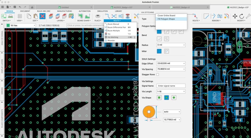
Implementing via stitching in PCB design requires careful planning and precision. Stitching vias involves locating and placing an extensive array of Vias around a board, with precise spacing. Stitching involves placing vias to improve grounding, reduce EMI, and enhance thermal management. Fusion offers utilities in their PCB Editor to place stitching vias with user-defined size and spacing, enabling designers to place stitching vias by selecting a via template or setting a custom Via size and layer transition.
PCB layout considerations
Achieving optimal performance in PCB designs requires meticulous attention to layout details, especially in managing ground planes and power planes. One of the most effective strategies is the use of stitching vias, which are strategically placed to connect copper areas across different layers. This technique involves arranging an array of vias—often along the edges of ground or power planes—with precise spacing to ensure a continuous grounding path. Stitching vias are crucial for reducing electromagnetic interference (EMI), as they help shield sensitive signal traces from external electromagnetic fields and maintain a consistent ground reference.
Besides their role in EMI reduction, stitching vias significantly contribute to heat dissipation. By providing a direct path for heat to flow from high-power or high-temperature areas to regions where it can be safely dissipated, thermal vias help lower thermal resistance and prevent signal distortion caused by excessive heat. Proper grounding, achieved through the thoughtful placement of stitching and thermal vias, is fundamental to maintaining signal integrity and minimizing noise. By considering layout factors such as the number, location, and spacing of vias, designers can create PCB layouts that not only reduce electromagnetic interference and thermal resistance but also enhance the overall performance and reliability of the board.
The impact of via stitching on via impedance
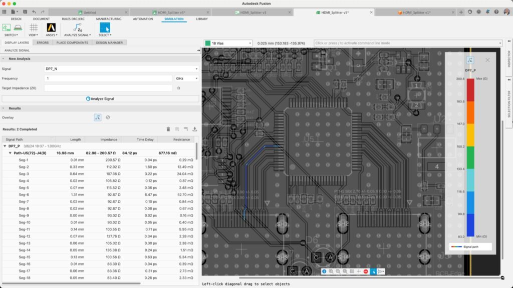
Via stitching and antipads work together to set the impedance of a via, both for single-ended signals and differential signals passing through vias. Vias connect multiple layers of the PCB, optimizing grounding and signal integrity in high-speed designs. Modifying the capacitance and inductance by the presence of a grounded stitching via near the signal via should be enough to suppress noise, particularly for slow GPIOs, I2C, UART, or other slow digital protocols.
Using via stitching in shielding
When you place viasStitching in an array, it can block electromagnetic waves up to certain frequencies, creating what many call ‘shielding.’ You should set the via spacing for shielding at approximately 1/10th of the wavelength of the highest frequency you need to shield from interfacing.
Via stitching for power
In a PCB layout for a power system, closely spaced Vias can provide high current with minimal temperature rise between layers. Via stitching is crucial for efficient power distribution and reliable power nets in high-current PCB designs, as it aids in managing current flow, reducing heat, and minimizing electromagnetic interference (EMI) across multiple layers. This would allow a Via to transfer large amounts of current with low loss between layers.
Automation of via stitching placement
Since the placement of stitching vias involves locating and placing an extensive array of vias around a board with precise spacing, automating this process can be a significant time-saver.
The role of via stitching in heat dissipation
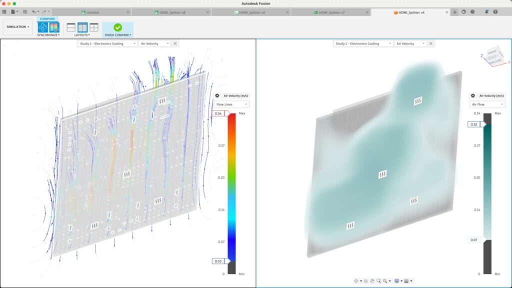
Via stitching also plays a critical role in heat dissipation. Via stitching on inner layers helps further improve heat dissipation and thermal management in high-power applications. When used near or under surface mount power components, via stitching spreads the heat to another, perhaps more significant, ground plane on the other side of the PCB, effectively reducing the overall junction temperature of the targeted high-power component.
Via stitching in multi-layer PCBs
In a multi-layer PCB, it’s common to have more than one region of copper assigned to the same ground net. Stitching vias are essential for ground plane continuity and thermal management in complex multilayer PCB designs. Stitching vias is a valuable tool for connecting these everywhere and ensuring the minimum possible impedance for any return current propagating along the reference plane in the PCB.
The impact of via stitching on noise reduction
The presence of a grounded stitching Via near the signal Via reduces noise in two ways. Firstly, the loop inductance in the Via region is lower because of being closer to the ground. Secondly, this proximity to the ground makes the signal via/ground Via transition dominate the total capacitance experienced along the Via.
In addition to noise reduction, via stitching also enhances the mechanical properties, mechanical stability, and mechanical strength of the PCB, making it more robust against physical stress and deformation.
The future of via stitching
The future of via stitching looks promising, with new advancements and applications on the horizon. As PCB requirements grow for higher efficiency and compactness, the role of via stitching becomes more critical. In addition, as PCB designs become more compact and complex, careful placement of stitching vias near critical components is increasingly important for ensuring both electrical performance and thermal management. As we push the boundaries of PCB design further, we can’t overstate the importance of mastering and applying via stitching in your designs.
In the grand scheme of PCB design, via stitching is just one of the many techniques available to designers. Yet, its impact is profound. via stitching provides significant benefits, such as improving ground return paths, managing ground loops, enhancing heat dissipation, and reducing noise. These advantages can significantly enhance your PCB designs’ integrity and performance. By mastering and applying this technique, you can elevate your PCB designs, ensuring they perform optimally and reliably for their intended functions.
Autodesk Fusion – your via stitching solution
Fusion includes advanced via stitching techniques to enhance the performance and reliability of their PCB designs. By strategically placing an array of vias to connect copper areas across multiple layers, Fusion ensures efficient power distribution and robust grounding. By integrating these sophisticated techniques, Fusion delivers cutting-edge solutions that meet the demanding requirements of modern electronic applications.