Get an in-depth look at the PCB layers in Fusion and understand how they help you track design data without cluttering your canvas.
If you’ve ever looked at the PCB layers list in Fusion and felt overwhelmed, then this post is for you! Layers are a critical component of your PCB design. They help you organize and keep track of key design data without cluttering your canvas. When you’re ready to generate documentation to share with your manufacturer, your Gerbers will pull data directly from many layers to communicate your design intent. There are 38 layers and remembering what they’re all used for can be a challenge. Let’s take a look at every layer in Autodesk Fusion and what you need to know about them.
Elevate your design and manufacturing processes with Autodesk Fusion
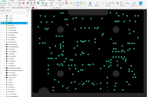
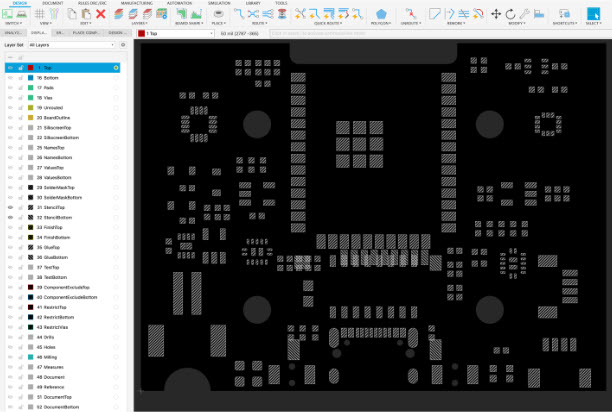
Layer 1 : Top
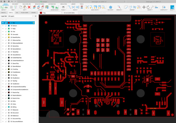
This first layer contains the copper on the top of your board, whether a polygon from a copper pour or individual copper traces. Using this layer to generate a pour will provide an accessible area of copper for all your signals to ground. Also, when creating pads for surface mount components, Autodesk Fusion will use Layer 1 for the pad’s placement. You can also adjust the angle of pads or components on Layer 1 to customize their orientation within the PCB layout.
PCB layers 2-15: Route
These PCB layers are primarily referred to as internal conductive layers on the PCB. Internal layers on the PCB can be used to route traces and copper planes. They have the same properties as the top and bottom layers. The primary difference is that traces or polygons created in the internal layers are not visible from the external layers. When your design has a high component count, you might run out of space to complete the PCB routing. In these situations, consider adjusting your layer configuration to include internal layers. This can dramatically increase your chances of successfully routing the entire board.
However, keep in mind that the cost of prototyping and manufacturing PCBs with internal layers increases significantly.
Internal PCB layers are frequently used as reference layers. These greatly enhance signal integrity on critical traces by providing dedicated ground and power planes. Internal layers are often used to create ground planes, which help reduce noise and improve signal integrity, especially in high-frequency designs.
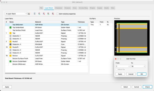
If you plan to design a multilayer PCB, how you orgranzie the top/bottom and middle layers will be slightly different. For example, creating a 4-layer board won’t just use layers 1, 2, 3, and 4. Instead, Fusion will use Layers 1 (top), 2, 15, and 16 (bottom) to bring it all together.
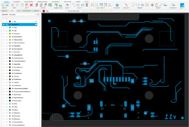
Layer 16: Bottom
This layer contains the copper on the bottom of your board, whether from copper pours or individual copper traces. Components on the bottom of your board will also have their pads placed here.
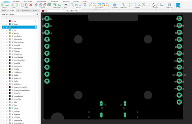
Layer 17: Pads
Here, you’ll find all your through-hole pads, including the hole on the copper surrounding it (Annular Ring). An annular ring will be placed on both the top and bottom layers of your board when placing a pad on this layer. You’ll rarely need to tinker with this layer, as through-hole pads are generate automatically once you put down a through-hole package.
You can also select different pad shapes, such as square, to specify the overall size and geometry of the pad and hole for soldering and electrical connections.
Layer 18: Vias
This is the layer for all your vias, providing a connectivity path for signals between layers on your PCB. Note that both vias and through-hole pads will look nearly identical. It’s always helpful to hide/show just Layer 18 or 17 to understand what specific object you’re viewing.
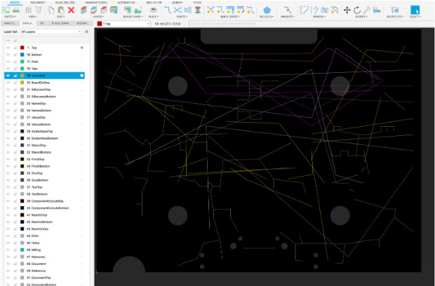
Layer 19: Unrouted
When you start a PCB layout, all your components connect with air wires, also called a rats nest. These lines specify connectivity between all of the pins on your components, and these lines live on the unrouted layer until they get connected. When you fully route your PCB, you should no longer have any visible unrouted wires. As you complete your routing, you can delete any unnecessary or stray lines to ensure a clean and accurate PCB layout. Follow this link to learn how to assign colors to your Signals/Traces and Net Classes.
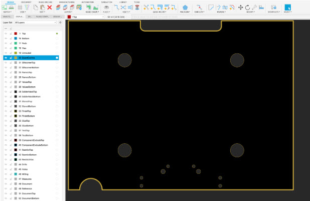
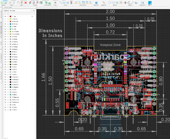
Layer 20: BoardOutline
The BoardOutline layer has several purposes, the first of which is to specify the outline of your board. You can also use this layer in your design rules to keep copper pours away from the edge.
This layer is also used in fabrication and assembly drawing outputs to clearly define the board’s shape for manufacturing.
Some fab houses like OSH Park will use this BoardOutline layer to generate a board outline for Gerber. This will serve as the exact shape of your PCB when they cut it into a fabrication panel.
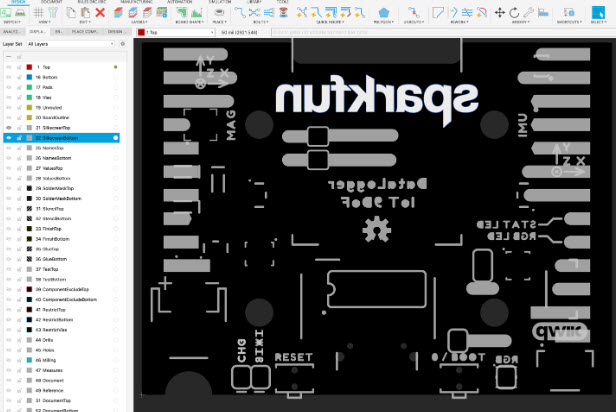
PCB Layers 21-22: SilkScreenTop/SilkScreenBottom
These two layers contain the top and bottom silkscreens on your PCB, which include the component outlines to show the positioning of parts. When using this layer, you must be careful not to place silkscreen on any soldered areas. Otherwise, you could risk malfunctioning on your board or creating an unsolderable pad.
If you need to place any documentation on your circuit board that will not be part of the manufacturing output, I recommend using the Document layers. For your convenience, the layer display will have them as layers 51 and 52.
Layer 51 is DocumentTop for top-layer documentation, and layer 52 is DocumentBottom for the bottom layer. These layers are not included in your manufacturing data export or printed on your PCB, so you can include many more details. However, if you want to add any artwork outside of the described regular silkscreen, like text or logos, then Layer 21-22 is the place to do it.
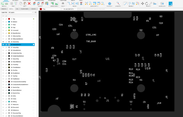
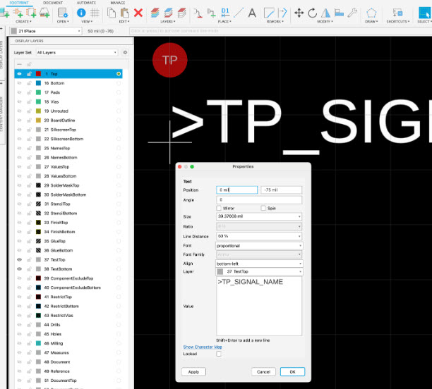
PCB Layers 25-26: NamesTop/NamesBottom
As the name suggests, these two layers contain the top and bottom print for your component names. Every component on your PCB has a unique name, also called a reference designator, and will look something like R1, C1, D1, etc.
You won’t need to worry about your component names, as they will automatically generate when you place them apart. However, arranging the names in the same orientation can be helpful to make your board more accessible to read and reference.
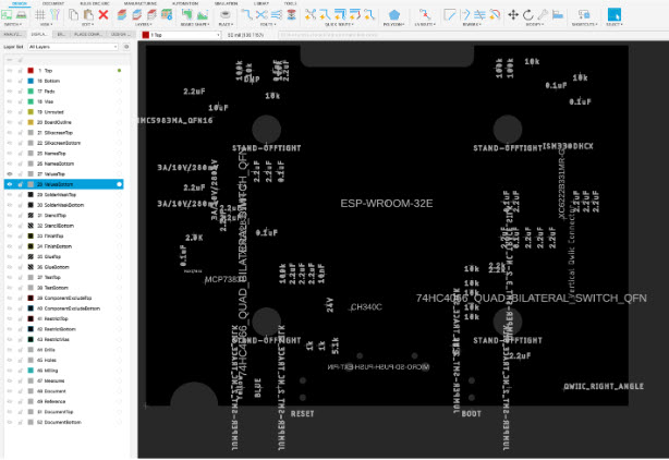
PCB Layers 27-28: ValuesTop/ValuesBottom
Again, as the name suggests, these two layers contain the specific values for every component on your board. For example, a resistor will have its particular resistance listed, maybe as 10K. Or, for a capacitor, you’ll see the capacitance listed, maybe as 0.1uF.
Many designers choose not to include this layer on their physical PCB. They opt to have a Bill of Materials (BOM) that they can reference by looking up the reference designator of a particular component. However, if you plan to design a PCB for a kit or hand-assembled board, it’s helpful to list both the component names and values on your PCB. This will make the assembly process a lot easier to digest.
PCB Layers 29-39: SolderMaskTop/SolderMaskBottom
These two layers indicate where you should not apply the solder mask. When placing either through-hole or surface mount components, these parts typically include a solder mask expansion area on these two layers.
Defining an area you don’t want a solder mask applied to will provide space on your copper for soldering parts. You can also use this layer to draw custom structures, like heatsinks or gold artwork, by exposing specific areas of copper.
PCB Layers 31-32: StencilTop/StencilBottom
These layers contain the solder paste data for your surface mount components. Your manufacturer usually uses this layer to make stencils for printing solder paste before assembling any parts.
This cream information will automatically generate for you when placing SMD packages. However, if you need to make an SMD footprint, add the cream area smaller than the solder mask so the two materials don’t overlap.
PCB Layers 33-34: FinishTop/FinishBottom
These two layers include data about any kind of unique finish that your board requires, like plated gold or silver carbon. It can also include data about specific pads that need immersion gold plating.
Remember, this layer will not generate automatically. You’ll need to draw it yourself if you need a special finish added to your board. However, if you’re starting with PCB design as a hobby, you likely won’t use this layer as a special finish, which can be expensive.
PCB Layers 35-36: GlueTop/GlueBottom
These two layers include the top and bottom sides of your glue mask. This mask helps secure components to your board that you expect to encounter stress during daily use, such as switches, jacks, or connectors.
Your manufacturer typically applies glue with one dot in the center of smaller components and a few dots under more significant parts like Integrated Circuits (ICs). Like the finish layers, you’ll need to draw this layer by hand if you need glue applied to specific areas on your board.
PCB Layers 37-38: TestTop/TestBottom
At the end of fabrication (creating your bare board) and assembly (stuffing parts on your bare board), your PCB will be thoroughly tested for any short circuits. These two layers play their role by providing dedicated test points on both the top and bottom of your PCB for bare board testing or ICT (In-Circuit Test) equipment.
Autodesk Fusion has a library called testpad.lbr, which contains test pads that you can quickly place on your board. These test points are available as specific footprints, allowing you to accurately place and organize them on your PCB for reliable testing and assembly. You’ll find a variety of test points you can add for through-hole and surface-mount components.
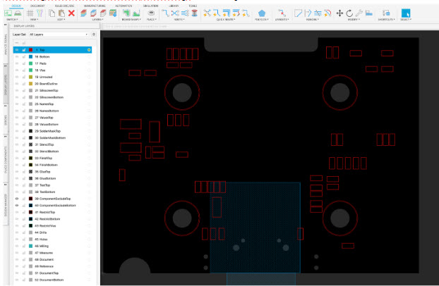
PCB Layers 39-40: ComponentExcludeTop/ComponentExcludeBottom
These reference PCB layers are intended to document that components should not be placed on these areas of the PCB. In other programs, these layers are known as courtyards. These features guarantee that components are too close. If an overlap on these layers is detected it indicates that components are too close together.
Maintaining proper spacing between components is crucial for the performance and reliability of electronic devices that use PCBs.
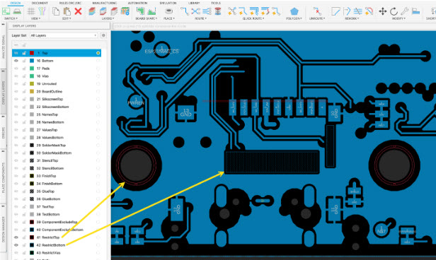
PCB Layers 41-42: RestrictTop/RestrictBottom/RestrictVias
RestrictTop and RestrictBottom indicate where traces or copper should be removed on your board layout. By default, when you fill in a polygon with copper over a restrict layer, the restricted section will remove any copper on the corresponding layer.
This layer also comes in handy when using the autorouter in Fusion. It can prevent traces from being routed in defined areas. Using restrict layers can help prevent trouble with routing constraints and ensure that traces and vias are placed only in appropriate areas. RestrictVia will indicate where vias should not be placed, and this layer will also prevent the autorouter from placing vias in defined sections.
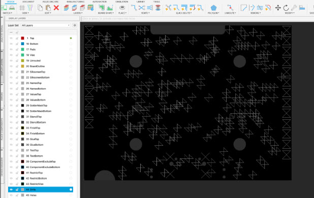
Layer 44: Drills
This layer contains all of the data for drills on your board that need to conduct electricity, such as through-hole pads and vias. This layer can also be helpful if you need to place a hole for a grounding bolt that will connect to your chassis.
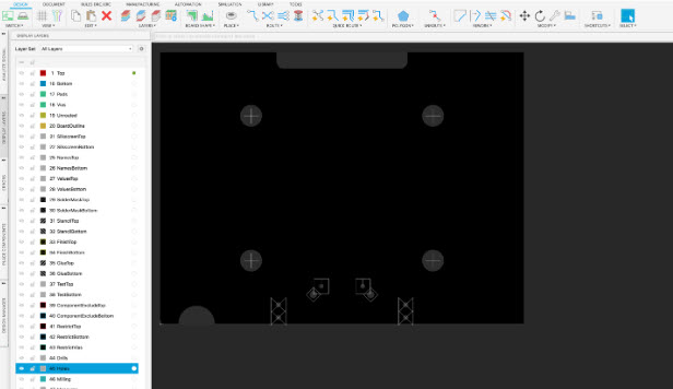
Layer 45: Holes
This layer is similar to drills but contains all of the data for holes that don’t need to conduct electricity, like unplated mounting holes.
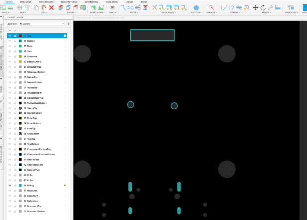
Layer 46: Milling
This layer is solely dedicated to milling holes, inner cutouts, and any other kind of contour that needs to be cut by your manufacturer. This layer is not meant to define the dimensions of your board. You’ll need to keep that data on Layer 20. And unlike the Board Outline layer, which can interact with your design rules, the Milling layer does not.
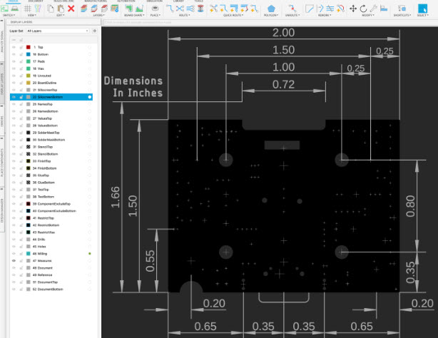
Layer 47: Measures
This layer contains all the measurements you need to make on your board, like the dimensions of your board outline or the spacing between components. Remember, this layer is meant for your reference and will not be part of the data sent to your manufacturer.
Layer 48: Document
This is the layer for all the supplementary documentation on your PCB. We recommend adding manufacturing notes on this layer for things like:
- Your PCB thickness
- Your layer stackup requirements
- Your solder mask and silkscreen colors
- Your desired copper type and weight
- Your impedance control specifications
- And your special finish requirements, if any
Layer 49: Reference
This layer contains the reference marks for fiducials on your board. Have you never heard of these? Little marks are placed on your PCB on the top and bottom layers that allow a machine to locate where your board is in physical space. At a bare minimum, we recommend including at least 2 marks on your design, but most manufacturers prefer 3.
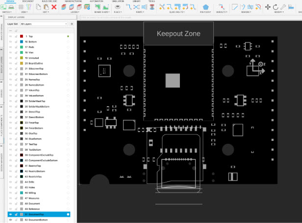
PCB Layers 51-52: DocumentTop/DocumentBottom
Last, we have the two documentation layers for the top and bottom of your PCB. These PCB layers will not be included in your manufacturing files but are handy details to include when referencing or reviewing your design.
You can also add screenshots or window captures of configuration dialogs to these documentation layers, providing additional reference for your design setup.
Manufacturing and assembly
Once your PCB design is complete in Fusion, the next step is manufacturing and assembly. This process starts by exporting your PCB layout as Gerber files—these are the industry-standard files that communicate your design intent to the manufacturer. Fusion makes it easy to generate these files, so that every layer, pad, and trace is accurately represented.
Choosing a reputable manufacturer is crucial for producing high-quality PCB boards. The manufacturer will use your Gerber files to fabricate the physical board, following your specified layer stack, copper weights, and other design details. After the PCB is manufactured, the assembly process begins. This involves placing and soldering electronic components onto the board, either by hand for small batches or with automated machines for larger runs.
Proper assembly is essential to ensure that all components are correctly connected and that the board functions as intended. By understanding the manufacturing and assembly process, you can create PCB boards that are not only well-designed in Fusion but also reliable and ready for real-world applications.
Collaboration and review
Collaboration and review are key to successful PCB designing, especially when working on complex projects or as part of a team. Fusion streamlines this process by allowing multiple users to work on the same project simultaneously. This means you can easily share your PCB design, get feedback, and make improvements in real time—no more emailing files back and forth or worrying about version control.
Fusion also offers built-in tools to help you review your PCB layout. The design rule checker scans your board for common issues, such as incorrect hole sizes, missing connections, or violations of spacing rules. This helps catch errors early, saving time and reducing costly mistakes during manufacturing.
For those looking to improve their skills, Fusion provides a wealth of tutorials and videos on YouTube, covering everything from basic PCB layout to advanced routing techniques. These resources are invaluable for both beginners and experienced developers looking to refine their electronics design process.
Finalizing the design
Finalizing your PCB design in Fusion is all about making sure every detail is correct before sending your files to the manufacturer. Start by double-checking your design settings—verify your layer stack, pad sizes, and component placements to ensure everything matches your project requirements. Fusion’s extensive libraries make it easy to find and use the right components, and you can even import files from other tools like Eagle if you’re working with existing designs.
When you’re ready, use the “Create” panel to generate your Gerber files. These files contain all the information your manufacturer needs to produce your PCB, including copper layers, solder masks, and silkscreen details. Make sure to review the generated files for accuracy, as even small mistakes can lead to manufacturing issues.
Fusion’ss flexibility allows you to export, import, and manage files efficiently, making it simple to create a complete and correct PCB design. By following these steps, you’ll be confident that your board is ready for the next stage—manufacturing and assembly.
Gotta catch em’ all
There you go, every single layer in \Fusion and what you need to know about them! Keeping track of all these layers might seem overwhelming at first, but as you dig into the intricacies of PCB design, you’ll see just how handy it can be to have this information available. Of course, we also can’t forget how much of the data in your layers will be shipped to manufacturing. We’re talking about things like the dimensions of your board, copper pour areas, silkscreen, reference designators, and much more.
\Fusion’s layer capabilities are designed with you in mind! They are logically named and include a customizable display panel that is always available, ready to help you switch views quickly and easily, streamlining your design process.
Fusion allows you to start your PCB design from scratch, giving you full control over every aspect of your project. You can easily search through component libraries to find and add the right parts to your design. Setting up a new device in your project is straightforward, with clear options for naming and connecting hardware components.
Try it today and see how Autodesk Fusion can help you bring your next product design to life sooner!