Fusion Fusion
Overview
Solutions Back
  • Manufacturing
  • Consumer Product Development
  • Mechanical Design
  • PCB and Circuit Design
  • Data Management
Plans and Pricing
Download free trial
See Autodesk Fusion pricing
  • All
  • Thought Leadership
  • What's New
  • Tutorials
  • Case Studies
  • Product Design & Engineering
  • Manufacturing
  • Electronics Engineering

Edwin Robledo

I began my career in the communications industry, primarily with the implementation of fiber optics communications and data management. I joined the EAGLE team 25 years ago to satisfy my passion for being involved with circuit board designs. I’m the Technical Marketing Engineer for Fusion 360 electronics and part of the Fusion 360 community team. I have published best practices articles, Blogs, hundreds of video tutorials, and hosted several electronic design bootcamps. My passion is anything related to the outdoors, especially outdoor photography and hiking.
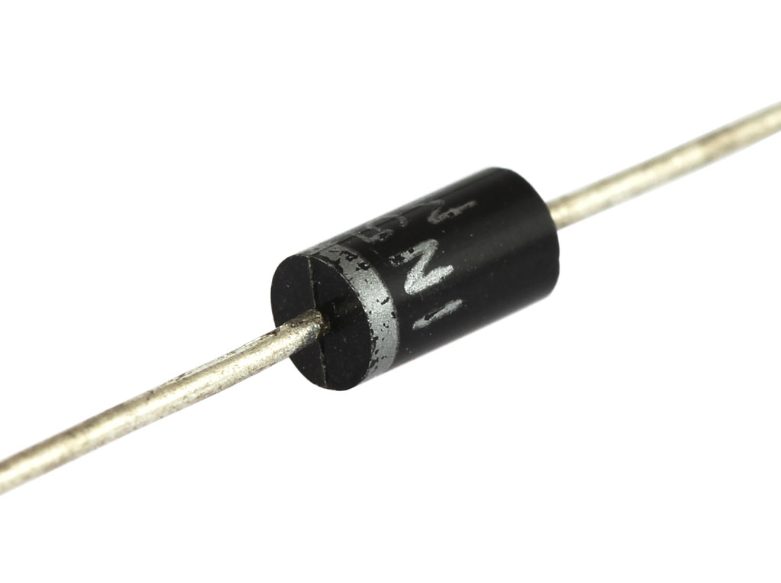
  • Diode Polarity & Symbols Explained

    Learn how the diode works to control the flow of electric current in a circuit with the use of n-type and p-type semiconductors.

    Electronics Engineering


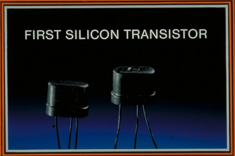
  • How Transistors Changed Electronics Forever

    Learn about how TI and Bell Labs changed electronics forever by inventing transistors.

    Electronics Engineering


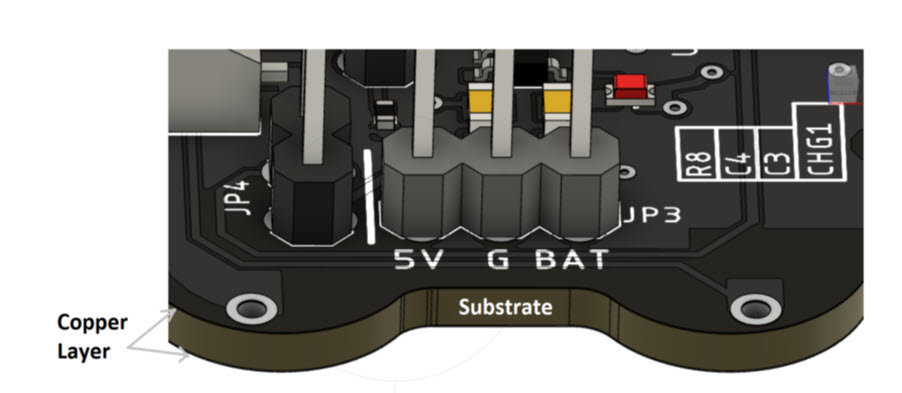
  • PCB Layer Stack Fundamentals: PCB Substrate

    In this 3-part series, we'll talk PCB substrates. Learn what a PCB substrate is, its physical specifications and why they matter.

    Electronics Engineering


  • Everyday App Note: How to Perform a Noise Analysis on Any Op Amp Circuit

    Learn how to perform noise analysis on any op amp circuit in today’s Everyday App Note!

    Electronics Engineering


  • It’s as Easy as Running – Understanding Voltage, Current, Resistance, and Ohm’s Law

    Learn all about how to measure and manipulate a circuit in your electronics design with voltage, current, resistance, and Ohm’s Law.

    Electronics Engineering


  • PCB Layer Stack Fundamentals: Routing Between Multiple PCB Layer Stacks

    Is there anything you should be aware of when routing between multiple PCB layer stacks? Let’s explore in this blog post. PCBs with multiple layers exist because it’s impossible to route today’s complex circuits on only one layer. This means eventually, the trace you’re routing will have to continue on another layer. Let’s explore everything…

    Electronics Engineering


  • PCB Layer Stack Fundamentals: Using Multiple Copper Layers

    In this blog post, we’ll examine the things to watch out for when using multiple layers of copper for your PCB layer stack.

    Electronics Engineering


  • Meet Ross Freeman, Inventor of the First FPGA

    Although his life was cut tragically short, Ross Freeman accomplished incredible things in life, including inventing the first FPGA.

    Electronics Engineering


  • How Thomas Edison’s Invention Factory Pioneered Team Collaboration

    Thomas Edison’s invention factory brought great minds together, creating a collaborative model still widely used today.

    Electronics Engineering


  • How to Use Thevenin’s Theorem

    Learn how to use Thevenin’s Theorem to calculate current and voltage across a load resistor in a linear circuit.

    Electronics Engineering


  • Interactive Routing with Fusion 360 Electronics

    Learn how Autodesk Fusion 360 provides you with the necessary routing tools and environment settings to make interactive routing easy and efficient.

    Electronics Engineering


  • 10 Things Everyone Needs to Know About PCB Designers

    Learn the 10 things you need to know about PCB designers, the electronics design process, and how we design printed circuit boards.

    Electronics Engineering


  • ECAD/MCAD Collaboration: 3 Reasons Why Every Electronics Designer Needs MCAD Software

    We’re all designing products now — not just PCBs. Collaboration with MCAD is now a necessity. Do you have the tools to keep up?

    Electronics Engineering


  • 5 Reasons Why PCB Designers Need 3D Modeling Software

    PCB design revisions used to be costly and time-consuming. Not anymore! Here's why PCB designers need 3D modeling software.

    Electronics Engineering


  • The History of PCBs from 1870 to Today

    Learn about the history of PCBs evolution with the introduction of the transistor, integrated circuit, BGA, and SMT.

    Electronics Engineering


Previous Page
1 … 3 4 5 6 7
Next Page

Autodesk

Company overview
Careers
Investor relations
Autodesk Trust Center
Newsroom
Diversity and belonging

Autodesk Foundation
Sustainability
Contact us
Students and educators
Affiliate program
Autodesk Research
Design & Make with Autodesk

How to buy

View all products
Buying with Autodesk
Renewal options
Find a reseller
Sales and refunds
Choose your subscription plan
Pay as you go with Flex

Support

Product support
Manage your account
Download and install software
Autodesk Product Status
Education support
Contact support

Privacy | Do not sell or share my personal information | Cookie preferences | Report noncompliance | Terms of use | Legal | © 2024 Autodesk Inc. All rights reserved