This article dives deeper into the practical ways to map 3D models to your electronic components directly from a PCB schematic.
While the library assignment method remains the most sustainable for long-term management across various designs, there are times when a quicker, more immediate approach is required. This can often be the case with non-standard components or hardware, such as screws and fasteners, where they may not be part of your standard library.
Elevate your design and manufacturing processes with Autodesk Fusion
Direct mapping offers a swift solution, providing a realistic visual representation without needing a library assignment. It’s a nuanced yet flexible method that fits PCB design’s fast-paced and often unpredictable nature. For a more detailed understanding and step-by-step guidance in 3D mapping in the library editor, please consider revisiting the initial blog where these concepts were first introduced and methods explained.
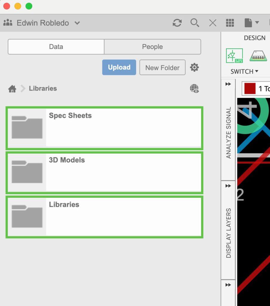
Setting up your project: Libraries, specification sheets, and 3D models
TIP: I recommend creating a project before we begin where you can store all your libraries. This will allow us to provide a step-by-step explanation. This project should consist of 3 folders: one for Libraries, one to upload specification sheets, and another for 3D models. You can draw the 3D models with Fusion or upload them from a reliable source in the form of a step file. This will make it so much easier to manage your libraries, especially if you plan to share them across teams.
Navigating the package editor workspace and initiating direct mapping
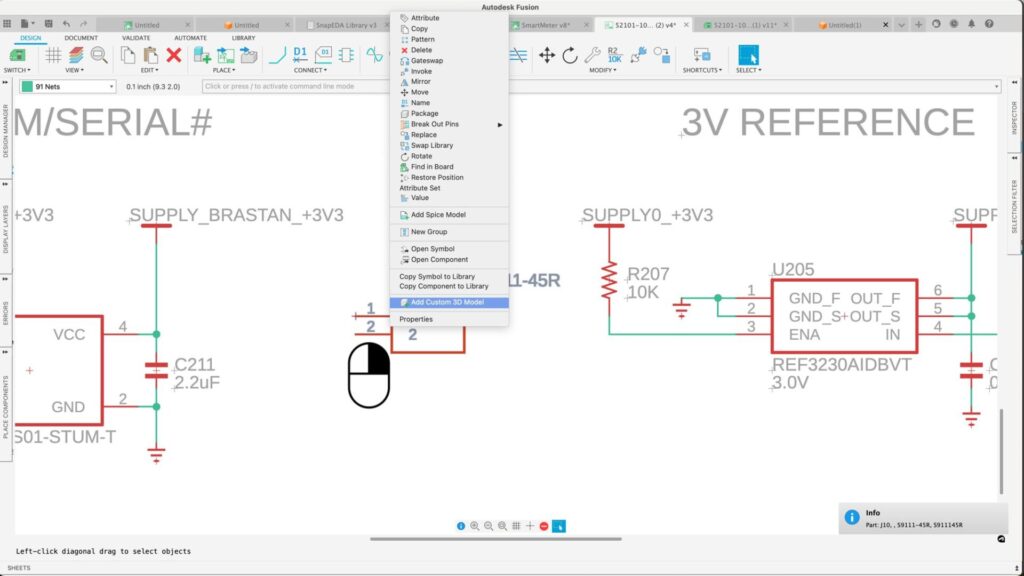
The Package Editor workspace in Autodesk Fusion is where the process of 3D modeling for electronic components happens. Its robust capabilities allow you to map STEP files to your 2D footprints or create a 3D model using one of the many IPC-compliant calculators at your disposal. As discussed in our introductory blog, we’ve previously navigated to the Package Editor through the library editor. In this session, however, we will approach the Package Editor via the Schematic or the PCB for a more direct mapping process. Let me take you through mapping a 3D model right from the Schematic.
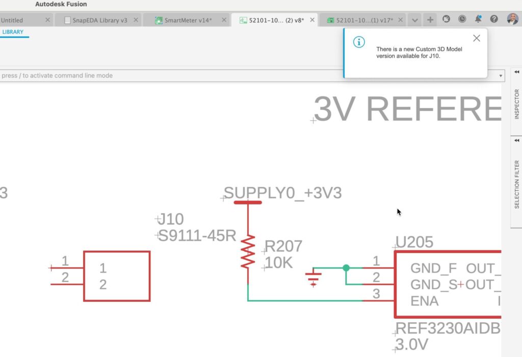
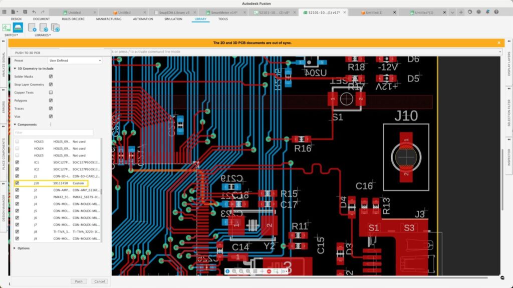
There are a few ways to find out which assets on your design do not have a 3D model. I will cover both of them. In the PCB layout editor, push to create a 3D model of your PCB. Notice that the Push to 3D dialog box will list all the electronic components of the PCB. The components that don’t have a 3D model will appear on the top of the list with an Alert symbol next to the footprint name. The ones that don’t have a 3D model will appear on the top of the list with an alert symbol. Notice that the J10 wire connector has an alert indicating that it is missing a 3D Model.
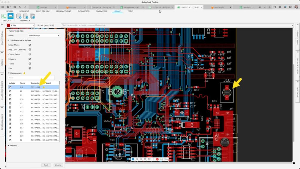
If you push our design to 3D as is, you will see that a default box represents the package. The component outline determines the size of this box.
Mapping a 3D model: Step-by-step guidance
Let’s return to the schematic and go through the steps to map this top-entry socket made by Harwin. I was able to get the 3D model for it from the Mouser distributor.
From the context menu, select the option to Add a Custom 3D Model.
As expected, this action will open the Package editor. The construction lines indicate the 2D Footprint; this will help to make sure we line up our 3D model correctly. Go to your Library/3D Model folder. Choose ‘Insert the 3D model to our design’ from the context menu. In this instance, we’re focusing on our 3D Modeling. You can either design 3D models for electronic components in Fusion or upload them from reliable sources like UltraLibrarian.com, SnapEDA.com, Findchips.com, Digikey, or Mouser.
With the 3D model inserted into the Package editor, let’s use the arrows to fine-tune the STEP 3D Model correctly. There are many options for this action; use the one that best accommodates you.
After selecting Finish, you will receive a message stating that the component has been successfully updated
Return to the PCB. You will notice there is a notification that there has been a change in the design and that it wants change in the design and it want to update the 3D model.
I would like you to notice that the Push to 3D dialog box no longer has the alert message regarding missing 3D models and that J10 has now been tagged with a Custom Model.
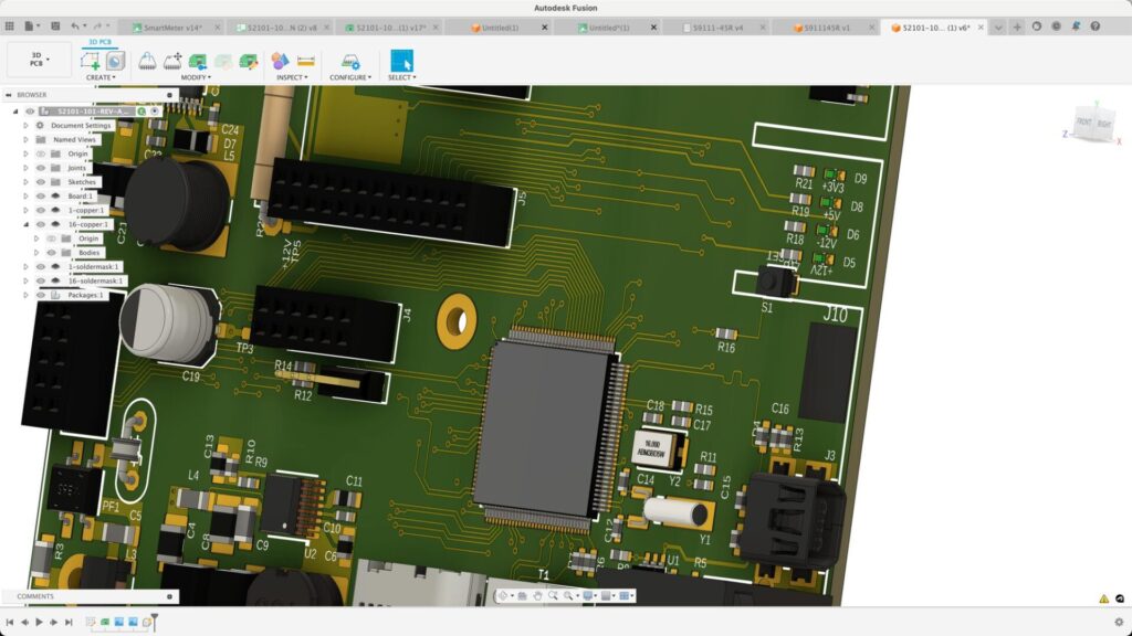
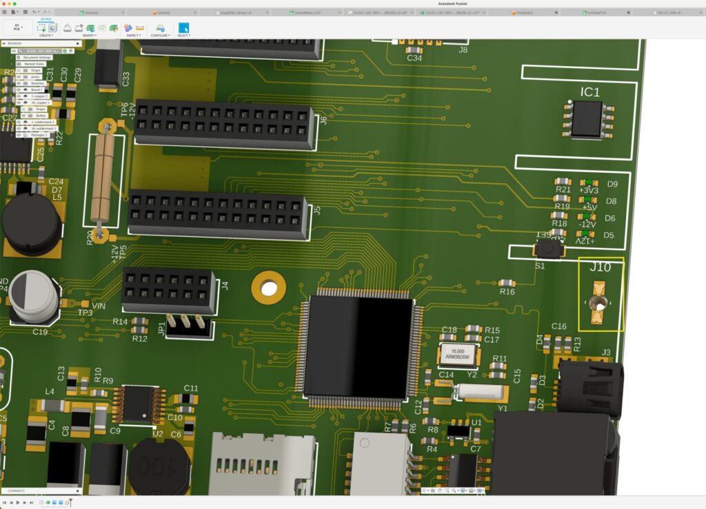
After selecting Push, in moments, the 3D model of your PCB will be displayed in the 3DPCB workspace with all components mapped, including our Socket J10.
As you can see, Fusion is very flexible, enabling you to map your 3D models from schematics so you can get to the market sooner. What are you waiting for? Try Fusion Electronics today.