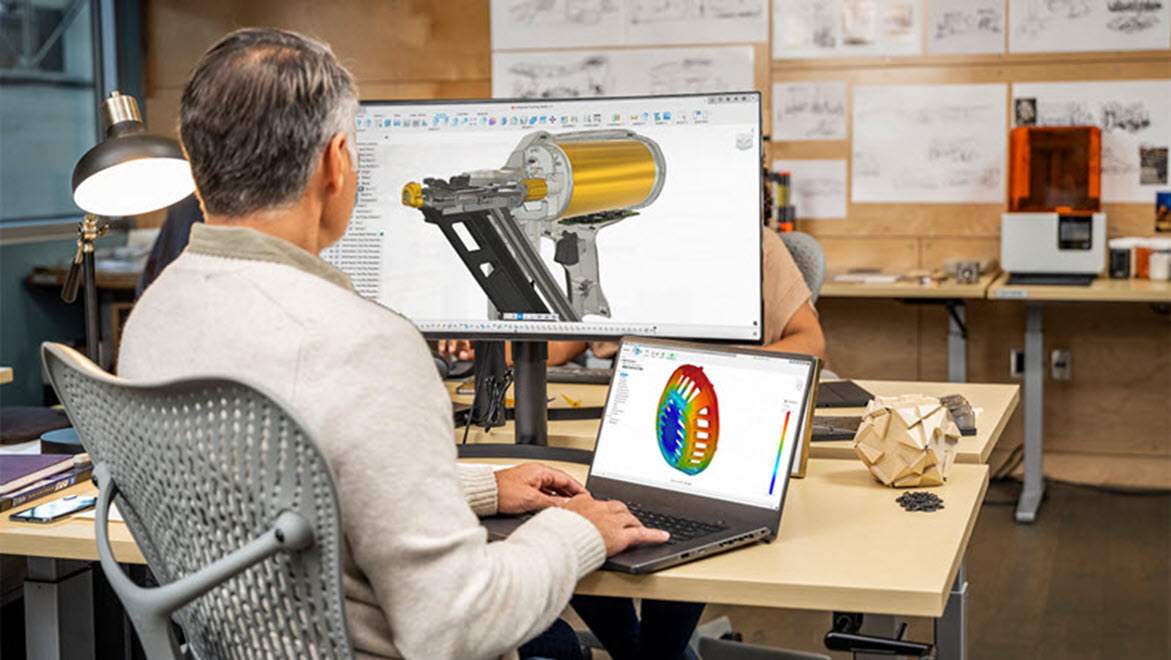
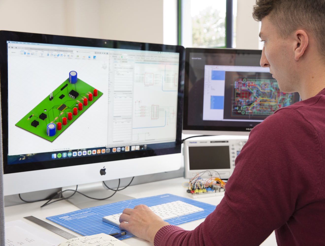
Discover how Autodesk Fusion and the Avnet add-in streamline electronics design with real-time data, seamless collaboration, and BOM optimization. Bringing innovative products to market requires more than just great ideas—it demands seamless collaboration, real-time data, and tools that bridge the gap between design and manufacturing. Autodesk Fusion, enhanced by the Avnet add-in, is redefining how…
Fusion
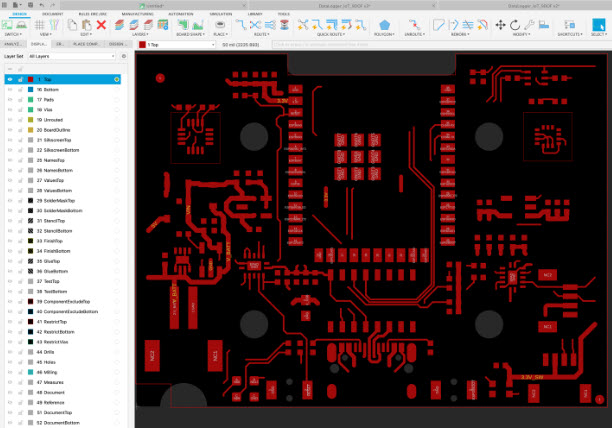
Achieve reliable PCB layouts with optimal trace spacing—learn expert strategies and use Autodesk Fusion for error-free, manufacturable designs. Printed circuit boards (PCBs) are the foundation of electronics, powering everything from smartphones to industrial machinery. Yet, one of the most critical, and often overlooked factors in PCB design is trace spacing: the minimum distance between conductive…
Fusion
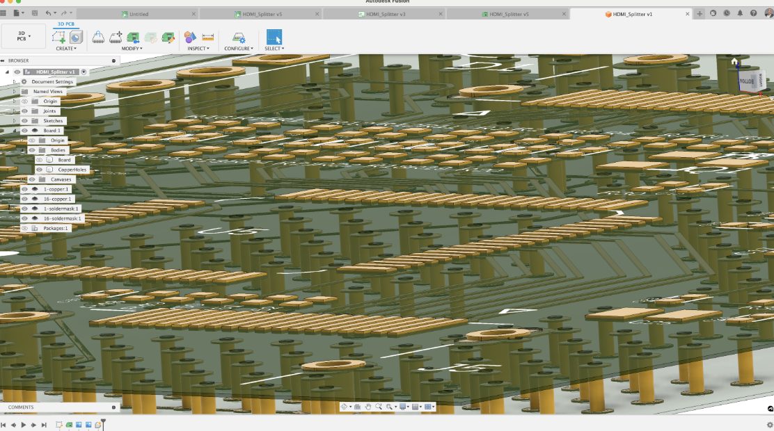
Explore the crucial role of Via Stitching in PCB design, its types, implementation, and benefits in enhancing performance, managing ground loops, and heat dissipation.
Electronics Engineering
Get an in-depth look at the PCB layers in Fusion and understand how they help you track design data without cluttering your canvas. If you’ve ever looked at the PCB layers list in Fusion and felt overwhelmed, then this post is for you! Layers are a critical component of your PCB design. They help you…
Fusion