
Modern EDA tools for PCB and electronics design
Modern EDA tools for PCB and electronics design
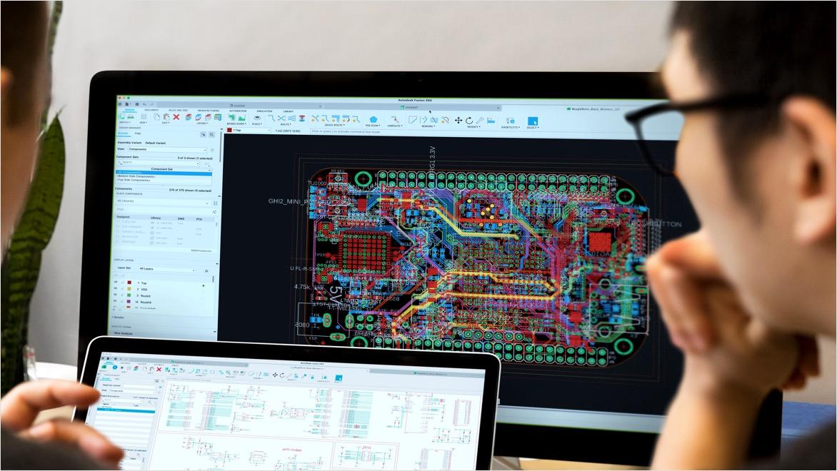
Why EDA software is essential for modern electronics design
Why EDA software is essential for modern electronics design
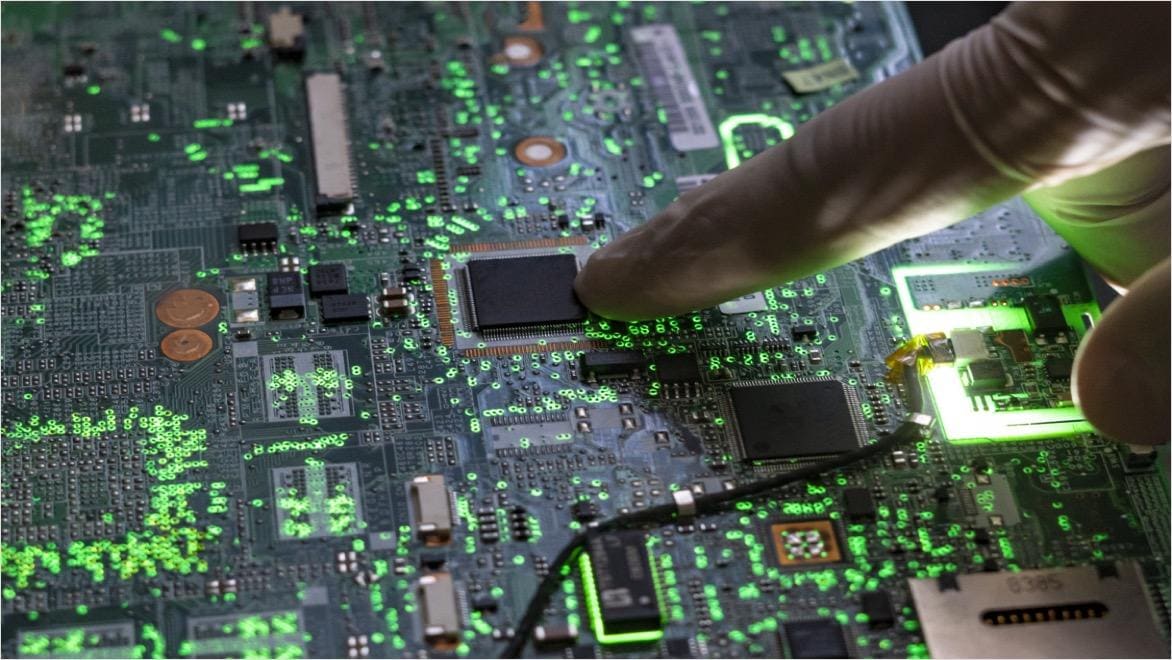
Autodesk Fusion for electronic design automation
Autodesk Fusion for electronic design automation
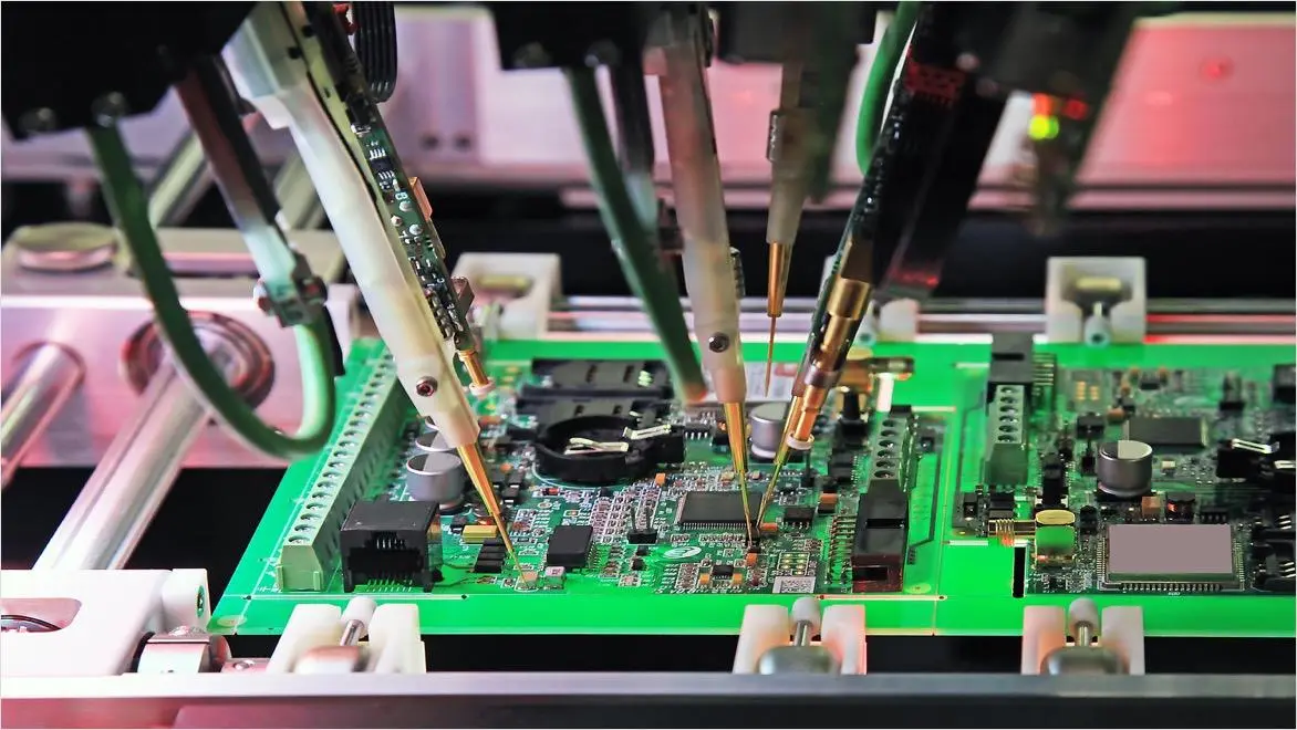
How electronic design automation software works
How electronic design automation software works
Manage design complexity
Manage design complexity
Improve accuracy and reliability
Improve accuracy and reliability
Increase engineering productivity
Increase engineering productivity
Reduce time-to-market
Reduce time-to-market
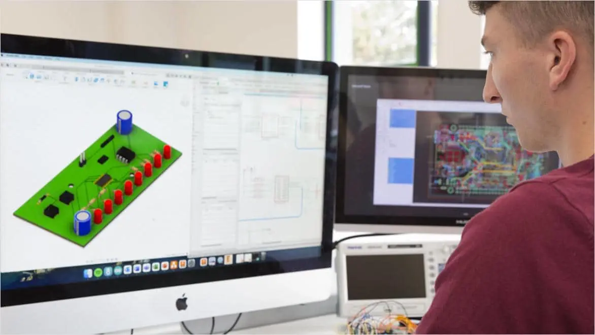
Emergence of EDA
Emergence of EDA
Future trends in EDA
Future trends in EDA
What is electronic design automation (EDA)?
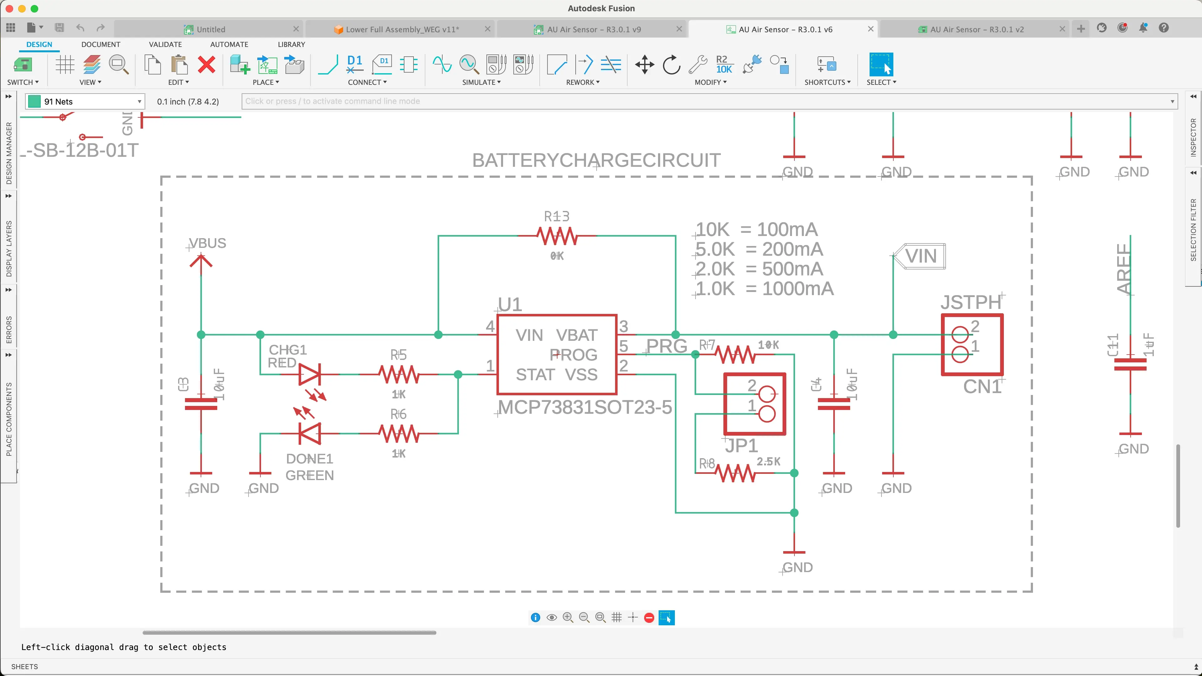
Electronic design automation (EDA) is a category of software used to design, simulate, verify, and manufacture electronic systems such as printed circuit boards (PCBs) and electronic circuits. Autodesk Fusion delivers EDA capabilities, enabling electronics design within an integrated product development platform.
What is EDA software used for?
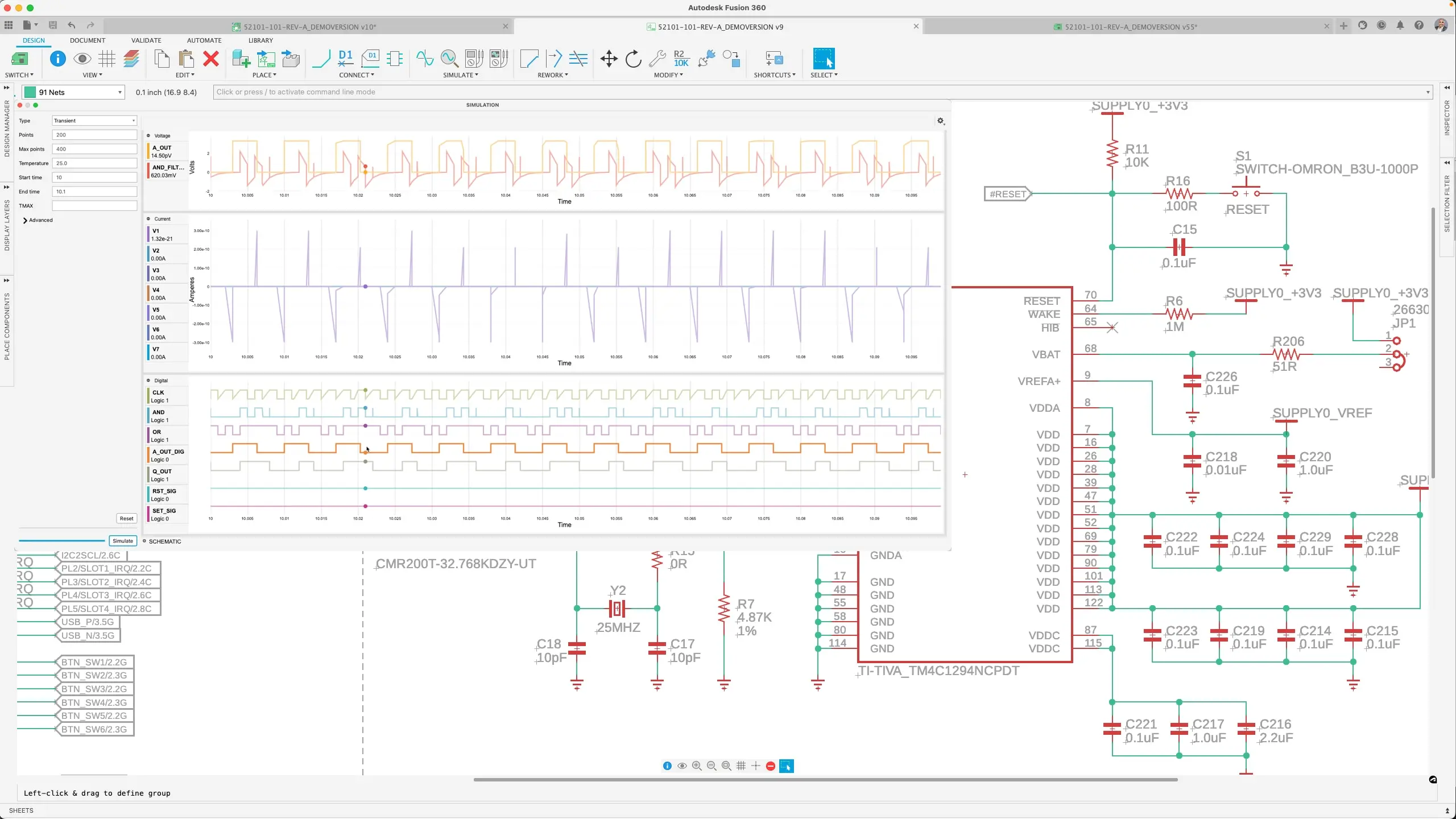
EDA software is used to create electronic schematics, design PCB layouts, run simulations, verify designs, and generate manufacturing outputs for electronic products.
In Autodesk Fusion, these EDA tools are available alongside mechanical design, helping teams streamline electronics development from concept to production.
What are EDA tools?
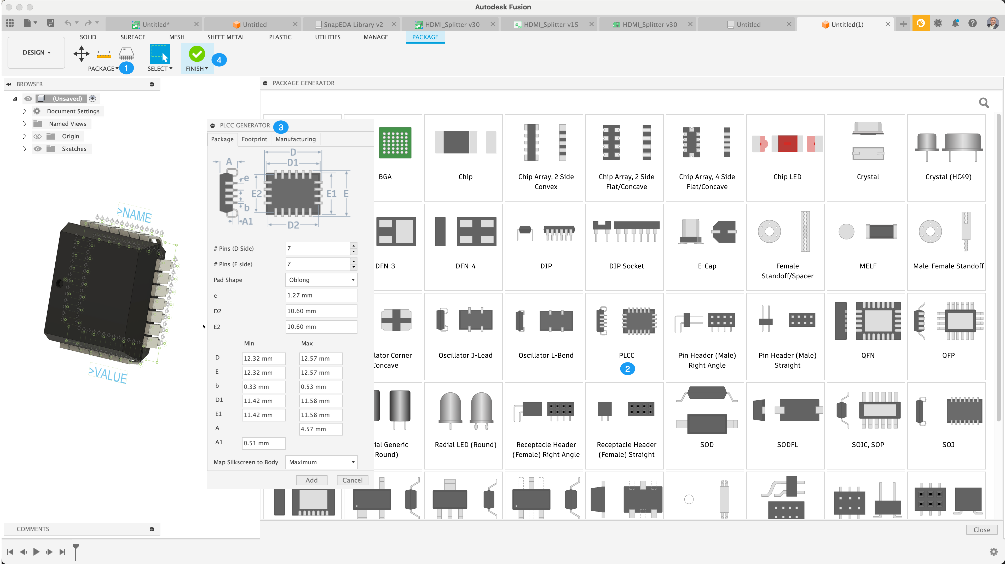
EDA tools are applications within electronic design automation software that support specific tasks such as schematic capture, PCB layout, simulation, and design rule checking. EDA tools are built directly into Autodesk Fusion, reducing the need for disconnected electronics workflows.
Why is EDA software important?
EDA software helps manage the complexity of modern electronic systems, improves design accuracy, identifies errors earlier, and reduces time‑to‑market. By using electronics design automation software, like Autodesk Fusion, teams can validate electronics designs sooner and reduce costly rework.
What industries use electronic design automation software?
EDA software is used across industries including consumer electronics, automotive, aerospace, telecommunications, industrial equipment, and medical devices.
What is the difference between EDA and ECAD?
EDA (electronic design automation) refers broadly to software for designing electronic systems, while ECAD (electronic computer‑aided design) is often used interchangeably and focuses on schematic and PCB design tools. Autodesk Fusion supports both EDA and ECAD workflows in a single environment.
What is schematic design in EDA software?
Schematic design is the process of creating a logical representation of an electronic circuit using standardized symbols and connections within EDA tools. In Autodesk Fusion, schematic design is connected directly to PCB layout and mechanical context for better design continuity.
What is PCB design in electronics design automation?
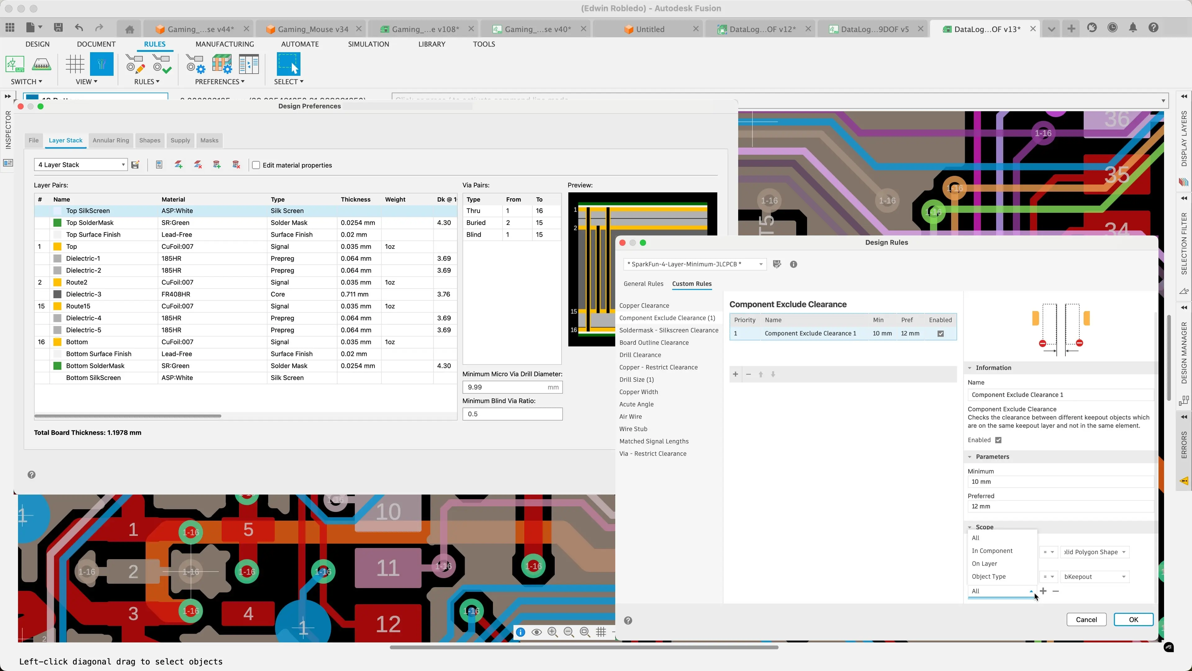
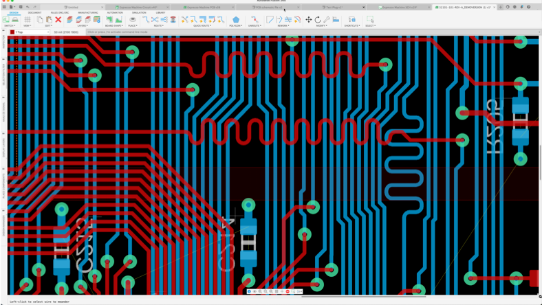
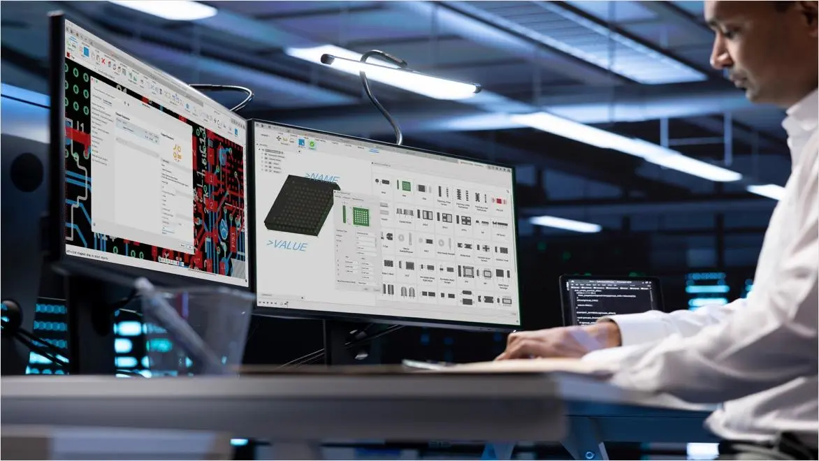
PCB design involves placing electronic components and routing connections on a printed circuit board while meeting electrical and manufacturing constraints using EDA software. Autodesk Fusion EDA tools support PCB design alongside 3D mechanical modeling to improve electronics‑to‑enclosure alignment.
Does Autodesk Fusion include EDA simulation tools?
Yes. Autodesk Fusion includes simulation and validation tools that allow engineers to analyze electronic designs and identify potential issues before manufacturing. Users can explore these capabilities through a Fusion trial.
How does EDA software reduce errors?
EDA tools use simulation, verification, and design rule checks to identify potential issues early in the design process, reducing costly rework later. In electronics design automation software like Autodesk Fusion, electronics design checks are integrated with the broader product model, helping teams reduce downstream errors.
Can EDA software support team collaboration?
Yes, electronics design automation software like Autodesk Fusion, supports collaboration by allowing electronics and mechanical teams to work from shared design data, improving visibility and coordination across disciplines.
How does Autodesk support electronic design automation?
Yes, Autodesk Fusion offers EDA tools for schematics, PCB layout, simulation, and electronics‑to‑mechanical collaboration in one platform.
Can I try Autodesk Fusion EDA software?
Yes. Autodesk offers a free 30-day trial of Fusion, allowing users to explore EDA tools, including schematic design and PCB layout, before choosing a subscription.